Comparative Optical Studies of Cu, Mn, and C Impurities in Bulk Lec grown GaAs by Electron Beam Electroreflectance (EBER
- PDF / 444,542 Bytes
- 6 Pages / 420.48 x 639 pts Page_size
- 96 Downloads / 305 Views
COMPARATIVE OPTICAL STUDIES OF Cu, Mn, AND C IMPURITIES IN BULK LEC GROWN GaAs BY ELECTRON BEAM ELECTROREFLECTANCE (EBER) AND PHOTOLUMINESCENCE (PL). M. H. HERMAN*, P. J. PEARAH**, K. ELCESS*, AND I. D. WARD* Charles Evans & Associates, Redwood City, CA 94063 Spectrum Technology, Holliston, MA 01746
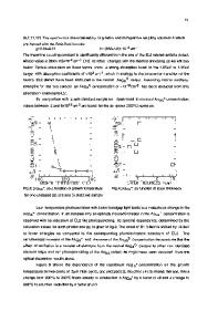
ABSTRACT We have used 300K Electron Beam Electroreflectance (EBER) and 4.2K photoluminescence (PL) to measure optical transitions in a series of LEC grown GaAs samples. The contaminants primarily consisted of the individual elements 16 3 Cu, Mn, and C at levels above 10 /cm . In unmodified control samples we find evidence of strong excitonic effects in the EBER lineshape even at 300K. For the contaminated samples, we find characteristic impurity transitions below the E0 bandgap of the GaAs in both optical spectroscopies. However, in general the estimated impurity binding energies by EBER are not equivalent to established PL or DLTS values. Specifically, from EBER data we find below E0 (1.424eV at 300K) a Cu peak near 49meV (1.375eV) and a C peak about 39meV (1.385eV) below E0 . An EBER spectrum of the Cu-contaminated sample at 124K shows an asymmetric Cu impurity peak 47meV below E 0. The C feature has been ascribed to either Si or Ge from corresponding PL energies by several earlier researchers. Two samples which had been implanted with Mn and annealed show a peak about 43meV below E0 (1.381eV), and what appears to be a sharp, excitonic transition 10 to 16meV above the E0 . Although these features may be due to Mn alone, the latter observation is suggestive of strain-induced valence band splitting. The correlated appearance of impurity peaks below the split-off E 0+AA0 band may allow their assignment to either donors or acceptors in modulated reflectance studies [1,2]. None of the present cases showed corresponding transitions below E0 +A0, suggesting that the observed impurity features arise only from acceptor transitions. Alternatively, the reduction of light penetration into the GaAs above the E0 bandgap, reducing the sample interaction volume, may also explain this null observation.
INTRODUCTION The detection and characterization of elemental impurities and crystalline defects in compound semiconductors by optical spectroscopies has been fundamental to the development of solid state technologies. Especially in the GaAs system, photoluminescence (PL) has been extensively researched for the purpose of characterization of impurities [3]. However, PL alone is not sensitive to all defect types and is often complemented with DLTS and Hall measurements for further investigations of electrically active levels which do not luminesce. Other optical spectroscopies are also used to supplement PL studies of GaAs, such as IR transmission for detection of the EL2 concentration near midgap, and those of the electroreflectance (ER) modulation spectroscopy family, which are increasingly used to assess both bulk crystals and epitaxial heterostructures [4]. The identification of impurities in ER spectra began with the earliest disco
Data Loading...