Correlation between Gate Induced Drain Leakage and Plasma Induced Interface Traps
- PDF / 579,520 Bytes
- 6 Pages / 415.8 x 637.2 pts Page_size
- 43 Downloads / 241 Views
117
Mat. Res. Soc. Symp. Proc. Vol. 592 © 2000 Materials Research Society
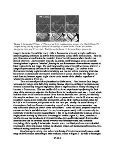
EXPERIMENTAL The devices used to evaluate the plasma charging damages were 20[im/0.4vm p+polysilicon gate p-channel MOSFET's with 50 A gate oxide. Different antenna structures were fabricated in metal I layer. An HP4156A parameter analyzer was used for device parameter extraction. Interface traps were measured using charge pumping technique [11]. The gate pulses, supplied by an HP8112A pulse generator, have a fixed high level Vh and varying base level Vb with 50% duty cycle, a frequency of 200kHz and a 50.Ons/V rise/fall gradient. During the charge pumping measurement, the trapezoidal pulse is applied to the gate, the substrate is grounded, and the dc charge pumping current is measured from either drain junction or the substrate while the source junction is left floating [Il]. This test configuration enables us to eliminate the contribution from the interface traps at the source junction and extract specific signal related to the interface traps at the drain side, which are responsible for GIDL enhancement. RESULTS AND DISCUSSION Fig. I shows the subthreshold characteristics for 20/0.4 ýtm p+/pMOSFETs with different antenna area ratio (AAR) in the same cell location. Compared with the reference device (with no antenna), there is a significant increase in GIDL current IGIDL in the devices with antenna structure. IGIDL magnitude increases with increasing AAR. In this paper, IGJDL is defined as drain current measured at the fixed condition of Vc = 0 V and VD =-3.3 V. In Fig. 2, the lGIDL magnitudes of p+ polysilicon gate pMOSFETs with different AAR (or different antenna length ratio (ALR)) are plotted as a function of cell location. Seven cells along a central line across the wafer were used for the measurement. It can be seen that lGwDL changes regularly according to the distance between the device site and the /
103
Do=-3.3V
..''.'' ..•
vo0ol V D=O.
1V
A
.
0
A A
ýA
A A A A
A
AAA
10"
Data Loading...