Effects of GaN Thin Layer on InGaN at Electrolyte-Semiconductor Interface for the Application of Photoelectrochemical Wa
- PDF / 478,991 Bytes
- 6 Pages / 612 x 792 pts (letter) Page_size
- 26 Downloads / 287 Views
Effects of GaN Thin Layer on InGaN at Electrolyte-Semiconductor Interface for the Application of Photoelectrochemical Water Splitting Katsushi Fujii1,2, Kayo Koike2, Mika Atsumi2, Takashi Itoh2, Takenari Goto2, Takafumi Yao2, Masakazu Sugiyama3, and Yoshiaki Nakano1 1
Research Center for Advanced Science and Technology (RCAST), The University of Tokyo, 4-6-1 Komaba, Meguro-ku, Tokyo 153-0043 JAPAN 2 Center for Interdisciplinary Research, Tohoku University, Aramaki Aza Aoba 6-3, Aoba-ku, Sendai, Miyagi 980-8578, JAPAN 3 School of Engineering, The University of Tokyo, 2-11-16 Yayoi, Bunkyo-ku, Tokyo 113-8656, JAPAN ABSTRACT Photoelectrochemical properties of nitride semiconductors are paid attention due to their possibilities of water splitting by visible light absorption. However, the photocurrent density of InxGa1-xN, which absorbs visible light, is usually lower than that of GaN, which has larger bandgap and absorbing only UV light. The reasons of this are thought to be the band-edge position at the semiconductor-electrolyte interface and the crystal quality. The conduction band-edge decreases with increasing of indium composition and across the hydrogen generation energy at around the indium composition of 0.2. This means that the hydrogen generation ability decreases with increasing of indium composition. Low crystal quality is obtained because the lower growth temperature of InxGa1-xN than that of GaN to achieve the indium incorporation. In order to improve the photocurrent density, band-edge energy control and quantum tunneling effect are tried using the structure of thin GaN layer on InxGa1-xN here. The effect for the photocurrent densities is also discussed. INTRODUCTION Nitride semiconductors are studied as working electrodes for photoelectrochemical water splitting [1]. Especially, many research groups pay attention to InxGa1-xN, which is one of the candidates of water splitting photo-illuminated working electrode using visible light [2-4]. This visible light absorption of InxGa1-xN is expected that the photocurrent density is higher than that of GaN. However, the photocurrent density of InxGa1-xN is lower than that of GaN currently. This is explained the following two ressons; (1) The InxGa1-xN conduction band-edge energy decreases with indium (In) composition [5], and finally across the hydrogen generation energy from water at around the In composition of 0.2. The conduction band energy being lower than hydrogen generation energy means that water splitting cannot occur without any bias. (2) Large number of defects in InxGa1-xN consumes the carrier generated by photo-illumination and reduces the photocurrent compare to that of GaN. The reason is believed to be that the growth temperature of InxGa1-xN is much lower than that of GaN in order to achieve the indium incorporation in the crystal.
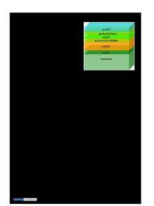
undoped GaN cap (0, 5, 15, 50 nm) n-type GaN:Si undoped GaN (0001) Sapphire (substrate)
undoped InxGa1-xN bulk (0.2 μm) Low temperature GaN buffer
Figure 1. Schematic sample structure of GaN cap layer on InxGa1-xN
Data Loading...