Effects of Thinned Multi-Stacked Wafer Thickness on Stress Distribution in the Wafer-on-a-Wafer (WOW) Structure
- PDF / 686,457 Bytes
- 6 Pages / 612 x 792 pts (letter) Page_size
- 55 Downloads / 350 Views
1156-D08-05-F06-05
Effects of Thinned Multi-Stacked Wafer Thickness on Stress Distribution in the Wafer-on-a-Wafer (WOW) Structure H. Kitada1, N. Maeda1, K. Fujimoto2, K. Suzuki2, T. Nakamura3 and T. Ohba1 1 University of Tokyo, 2-11-16 Yayoi, Bunkyo-ku, Tokyo 113-8656, Japan 2 3
Dai Nippon Printing, 250-1 Wakashiba, Kashiwa-shi, Chiba 277-0871, Japan Fujitsu Laboratories Ltd., 10-1 Morinosato-Wakamiya, Atsugi, Kanagawa 243-0197, Japan
ABSTRACT In the trough silicon via (TSV) structure for 3-dimensional integration (3DI), large thermal-mechanical stress acts in the TSV caused by the mismatch in thermal expansion coefficient (CTE) of the TSV materials. In this study, the stress of multi-stacked thin silicon wafers composed of copper TSV and copper/low-k BEOL structure was analyzed by the finite element method (FEM), aiming to reduce the stress of TSV of 3D-IC. The results of sensitivity analysis using design of experiment (DOE) indicated that the thickness of the silicon and adhesive layer are the key factors for the structural integration of TSV design. INTRODUCTION Since conventional downsizing based on an empirical Moore’s law has reached the limitations of manufacturability, performance, and power consumption, an alternative integration technology such as 3DI is needed. There have been many reports on 3DI involving many wafer bonding techniques [1-4]. The TSV, which is larger than the BEOL interconnects, is used for the interconnects in 3DI, But the large CTE mismatch of the adhesive material used for wafer bonding, Si substrate, and copper influence the stacked TSV structure. Recently, a roadmap for
(1)
(2) Metal-Pad Support glass Si substrate
Temporary adhesive
D. TSV etching
A. Thinning
TSV hole Photo-Resist
B. Bonding (wafer alignment)E. Side wall deposition SiN
C. Debonding
Permanent adhesive (CYCLOTENE) Base wafer
150µm 80µm
F. Metal filling & planarization TSV filled with Cu
7th 6th 5th 4th 3rd 2nd 1st wafer
Si substrate
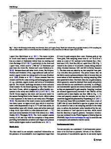
Fig. 1. (1) WOW process flow and (2) Seven-stacked thin wafers with TSV structure fabricated by the WOW process [6,7].
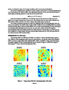
Fig. 2. FEM analysis model of 4-layer stacked Si with BEOL structure and copper TSV. the TSV diameter and aspect ratio of 3DI was presented by the ITRS. However, the roadmap approach is not suitable for adhesive material in 3DI because there are a lot of purposes such as logic/memoly, MEMS, and hetero device stacking. It was reported based on FEM thermal stress analysis around the TSV [5]. However, the influence of TSV stress that an aspect ratio has not been discussed in 3D-IC structures that use the adhesive. In this report, the sensitivity to copper stress of TSV aspect ratio and adhesive layer such as higher CTE was estimated by DOE using FEM analysis in order to eliminate the stress in TSV structures. EXPERIMENTS A novel through-silicon via (TSV) integration process formed after wafer bonding based on WOW has been developed [6,7]. The WOW process offers wafer-scale 3D manufacturability and high productivity of chip integration. Because the WOW uses
Data Loading...