Effects of Very High Workfunction Metals or Metal Alloys (NiCr) on High Switching Speed, HV Schottky Diodes for Mixed Si
- PDF / 1,126,583 Bytes
- 10 Pages / 432 x 648 pts Page_size
- 32 Downloads / 377 Views
MRS Advances © 2020 Materials Research Society DOI: 10.1557/adv.2020.336
Effects of Very High Workfunction Metals or Metal Alloys (NiCr) on High Switching Speed, HV Schottky Diodes for Mixed Signal or RF ASIC J. Pan, A. Gaibrois, M. Marripelly, J. Leung, S. Suko, M. Lee, T. Knight Advanced Technology Laboratory, Northrop Grumman Corporation,
1212 Winterson Road, Linthicum, MS 3A13, Maryland, 21090, U.S.A.
E-mail: [email protected]
Abstract. For high switching speed HV Schottky diodes, with very high work function metal and extremely lightly doped epi, the built-in potential may be too high for thermionic emission to occur, when the applied external voltage is quite low (near V F = 0.07V). If the epi is lightly doped p type, the built-in potential (VBuilt-in: potential difference between the metal and silicon Fermi levels) is 1.0V (measured with CV). If the external bias is 0.1V, near the measured VF, it is not enough to overcome the built-in potential for thermionic emission as illustrated. It is likely that in addition to thermionic emission, tunnelling and diffusion currents also contribute to the total HV Schottky diode forward current. TCAD simulation of HV Schottky diodes with N + guard bands suggests the potential barrier and electric fields at the Schottky junction are relatively high for thermionic emission to occur, when external bias V VF. In this paper we report HV Schottky diodes fabricated with various metals, metal alloys and epitaxial films. Metal work functions and epi doping profiles are extracted with high frequency CapacitanceVoltage (CV) technique. 150V of breakdown voltage and very low forward voltage (V F = 0.07V) are demonstrated. The measured data indicate very high work function metal or metal alloy is needed to achieve high switching speed and low forward voltage.
1
Downloaded from https://www.cambridge.org/core. Cornell University Library, on 17 Sep 2020 at 06:19:44, subject to the Cambridge Core terms of use, available at https://www.cambridge.org/core/terms. https://doi.org/10.1557/adv.2020.336
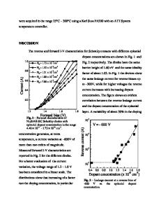
INTRODUCTION In the Advanced Technology Laboratory (ATL) at Northrop Grumman Corporation, high performance RF ASICs and power devices in silicon, GaAs, GaN and 4H SiC are simulated, designed, fabricated, and packaged. Extensive DC and RF tests are conducted. The performance of HV Schottky diode is superior to conventional p-n junction diode due to higher BV, lower reverse leakage, lower VF and higher output current [1] – [3]. We have fabricated HV Schottky Diodes. BV > 150V. VF = 0.07V. High breakdown voltage, low forward voltage drop, and low reverse leakage are achieved with very high work function metal alloys and low doping epi films. This is the first report proving very high work function metal alloys can be used to achieve < 0.1V of VF, with BV > 150V, and Schottky junction tunnelling is necessary to accomplish such high speed, high voltage goals, with suppressed thermionic emission effects. Modern Mixed Signal and RF ASIC demand both extremely high speed and the capability of
Data Loading...