Electrical and Optical Properties of 1 MeV-electron irradiated Al x Ga 1-x N
- PDF / 95,415 Bytes
- 6 Pages / 612 x 792 pts (letter) Page_size
- 92 Downloads / 328 Views
E11.35.1
Electrical and Optical Properties of 1 MeV-electron irradiated AlxGa1-xN Michael R. Hogsed1, Mo Ahoujja2, Mee-Yi Ryu3, Yung Kee Yeo1, James C. Petrosky1 and Robert L. Hengehold1 1
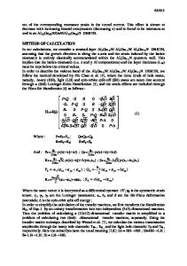
Department of Engineering Physics, Air Force Institute of Technology, Wright-Patterson AFB, Ohio. 2 Department of Physics, University of Dayton, Dayton, Ohio. 3 University of Dayton Research Institute, Dayton, Ohio. ABSTRACT The optical and electrical properties of Si doped GaN and Al0.20Ga0.80N films irradiated with 1 MeV electrons at a fluence of 1x1017 cm-2 are investigated using cathodoluminescence (CL), variable-temperature Hall-effect, and deep level transient spectroscopy (DLTS) measurements. The CL spectra measured at 6 K show peak luminescence intensity of the near band edge decreases, on average, by 50% after electron irradiation, indicating the creation of non-radiative recombination centers which are stable at room temperature. At room temperature, the free carrier concentration decreases significantly in both the GaN and AlGaN samples following the irradiation, and the carrier removal rate depends strongly on the initial carrier concentration. DLTS measurements show three electron traps in the as-grown Al0.20Ga0.80N. Following 1 MeV electron irradiation of the Al0.20Ga0.80N sample, three additional electron traps labeled R2, R3, and R4 are observed. The first two traps appear to correspond to radiation-induced traps reported in GaN while the latter appears to be unique to AlGaN. INTRODUCTION Group III-nitrides are of interest in the fabrication of high-temperature and highfrequency electronic devices as well as blue to UV light emitting and detecting devices [1-3]. Due to their robustness, they have long been regarded as being more tolerant to high energy particle radiation than is GaAs and other commonly used semiconductors. While much has been reported on the primary radiation-induced defect energy levels and the effect of radiation upon material properties such as carrier concentration, mobility, and luminescence efficiency in GaN over the past years, no such consensus exists for AlGaN material [4-8]. Of particular interest is to measure the radiation hardness of AlGaN/GaN devices for satellite based communications systems and nuclear industry applications. In this study, the electrical and optical properties of silicon doped GaN and Al0.20Ga0.80N irradiated with 1.0 MeV electrons at a dose of 1x1017 cm-2 are investigated using DLTS, variable-temperature Hall, and CL measurements. EXPERIMENT 1 µm thick AlxGa1-xN layers doped with silicon were grown by radio-frequency (RF) plasma assisted molecular beam epitaxy (MBE) on the C-plane of a sapphire substrate. The aluminum mole fraction was reported by the manufacturer based on CL and X-ray
E11.35.2
diffraction measurements. Prior to metal deposition, the AlxGa1-xN wafers were cut into small pieces of 5x5 mm2 each, degreased using standard chemical solvents, and followed by a dip in a boiling aqua regia solution for 30 s and a rinse in de-ionized water. For Ohmic c
Data Loading...