Electrical Hysteresis of PEDOT/PSS-Metal Contact Devices
- PDF / 112,363 Bytes
- 5 Pages / 612 x 792 pts (letter) Page_size
- 12 Downloads / 319 Views
I10.8.1
Electrical Hysteresis of PEDOT/PSS-Metal Contact Devices Zhengchun Liu, Yi Su* and Kody Varahramyan Institute for Micromanufacturing Louisiana Tech University Ruston, LA, 71272, U.S.A *[email protected] ABSTRACT: PEDOT/PSS is an air-stable and solution-processable semiconductor polymer with great potential for electronic applications. In this research, we investigated the PEDOT/PSS-metal contacts using Al-PEDOT/PSS-Au as a test device. Abnormal electrical hysteresis phenomena were observed in both the current-voltage and capacitance-voltage characteristics of the device. A model in terms of metal-polymer interfacial MIS structure and ion motion in the polymer is proposed for explanation of the ‘hysteresis’ phenomena.
INTRODUCTION Poly(ethylene dioxythiophene) doped with poly(styrene sulfonate) (PEDOT/PSS) is an airstable, solution processable semiconductor polymer. Recently, it has been intensively studied for electronic applications such as Schottky diodes [1, 2], organic light emitting diodes (OLED) [3], organic photovoltaic device [4], and organic thin film transistors (OTFT) [5]. In most of these organic electronic devices the metal materials are indispensable for their unique electronic properties. Therefore, to study the properties of metal-PEDOT/PSS contacts is of great significance to improve the device performance. In this paper, we investigated the electrical properties of metal-PEDOT/PSS contacts using Al-PEDOT/PSS-Au as a test device.
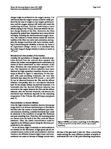
EXPERIMENTAL A silicon wafer is used as the substrate material. At first, a gold layer of 80 nm thick is deposited on the wafer by sputtering. Then, a film of PEDOT/PSS (Baytron P from H.C. Starck Inc.) is formed over gold layer using a drop-on-demand inkjet-printing technique. The average film thickness is 2 µm. The PEDOT/PSS film is cured at 120 ºC for 5 min in air. Finally, a 200 nm aluminum layer is deposited as top electrodes by thermal evaporation method using a shadow mask. The device structure is shown as the inset of Figure 1. The device area is 1.4 mm2. The devices are characterized on a Keithley electrical probe station system. Al electrode is biased and Au is grounded during the I-V measurement. During C-V measurement the voltage is only applied to Al electrode, too.
I10.8.2 3.00E-05 2.50E-05
Al PEDOT/PSS
2.00E-05 current (A)
1st sweep(-4V to 4V) 2nd sweep(4V to -4V)
III
Au Si
1.50E-05
II
1.00E-05
I
5.00E-06
IV
0.00E+00 -5
-4
-3
-2
-1
0
1
2
3
4
5
-5.00E-06 -1.00E-05 voltage (V)
Figure 1 The I-V characteristics (1st and 2nd sweeps) of Al-PEDOT/PSS-Au device. The first and second sweeps form two hysteresis loops. Inset is the schematic device structure. 1.50E-05 3rd 4th 5th 6th
current (A)
1.00E-05
sweep sweep sweep sweep
(-5 to 5V) (5 to -5V) (-5 to 5V) (5 to -5V)
5.00E-06
0.00E+00
-6
-5
-4
-3
-2
-1
0
1
-5.00E-06
2
3
4
5
6
Von
-1.00E-05
voltage (V)
Figure 2 The multi-sweep I-V characteristics of the same device as shown in Figure 1. The opposite voltage sweep can reduce the increased ‘turn-on’ voltage Von
Data Loading...