Electrochemical and Chemical Deposition of II-VI Semiconductors in Porous Silicon
- PDF / 1,043,281 Bytes
- 6 Pages / 414.72 x 648 pts Page_size
- 55 Downloads / 230 Views
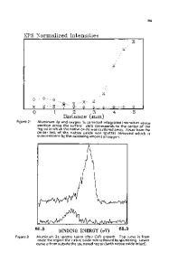
ABSTRACT The introduction of II-VI semiconductor compounds into porous silicon layers has been investigated in order to obtain transparent and conducting contacts with the inner surface of the material. CdTe and ZnSe have been electrodeposited cathodically on n type nanoporous electrodes from acidic solutions containing the metallic cations and dissolved oxides of selenium or tellurium. CdS incorporation into p-type porous silicon has been achieved by chemical bath deposition, from solutions containing cadmium complexes and thioacetamid as a sulfur donor. Characterization of the deposits has been performed by SEM observations, X-ray analysis and RBS. Results confirm the penetration of the compounds into the porous films, with small to strong concentration gradients in thickness depending on the deposition method. After deposition and sample drying, the luminescence of CdTe embedded layers has almost disappeared, whereas those containing ZnSe and CdS show a photoluminescence efficiency which is not severely degraded. INTRODUCTION Since the discovery of the photoluminescent [1] and electroluminescent [2] properties of porous silicon, many efforts have been devoted to the realization of bright emitting solid state devices based on this material, but despite recent significant progress [3-4], the electroluminescence efficiency remains quite low, in the order of 0.1%. However, bright electroluminescence with an efficiency similar to that of photoluminescence (near 1%) is easily observed when the electrical contact with the porous layer is achieved by means of a liquid electrolyte [5]. In such conditions, there is an intimate contact between the internal surface of the material and the electrolyte, allowing current flow through the whole structure. In the case of a solid contact, the conducting layer does not penetrate the pore network, so that it is only a part of the porous layer which electroluminesces. Moreover, as higher polarizations must be used, this results in quite strong electric fields in the material which reduce the radiative recombination rate [6]. Then, we believe that to get more efficient emission, it is necessary to realize a contact with the inner surface of the porous film. Several attempts have been made, either by filling the pores with a conductive polymer [7-8] or by electroplating metals [9], however such materials are not transparent in the wavelength range of the emitted light. Large band-gap 11-VI semiconductors seem to be better candidates to realize the contact with the porous layer: they can be chemically or electrochemically deposited, they can be chosen to be transparent in the luminescence speciral range, and they can form with silicon heterojunctions, which may lead to a good control of the charge injection into the nanocrystallites. In this preliminary work, we show that three different compounds can be successfully deposited into the porous layer, either by electrodeposition (CdTe and ZnSe) or by chemical 467 Mat. Res. Soc. Symp. Proc. Vol. 452 01997 Materials Research Society
bath
Data Loading...