Electron Beam Pumping in Nitride Vertical Cavities with GaN/ Al 0.25 Ga 0.75 N Bragg Reflectors
- PDF / 101,488 Bytes
- 6 Pages / 612 x 792 pts (letter) Page_size
- 5 Downloads / 339 Views
9W11.21
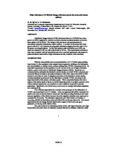
photonic excitation. The characteristics of the EBP emission spectrum depend on the electron beam intensity distribution, excitation time, penetration depth, etc. Realization of VCSELs relies on the fabrication of highly reflective mirrors, which could be produced by depositing suitable dielectric multilayers [4], resulting in several after growth processing steps. This can be avoided by integration of distributed Bragg reflector (DBR) stacks (made from multiple GaN/AlGaN/AlN layers) directly into the growth process, which also allows doping necessary for current injection. Many researchers have investigated DBR quarter wave stacks and achieved reflectivities of up to 96-97% at wavelengths in the blue-green and near UV spectral range[6-9]. We particularly focus attention on the two GaN/AlGaN DBR vertical cavity test structures. EXPERIMENT Our four DBR samples were grown by plasma assisted molecular beam epitaxy on sapphire (0001). On the first sample (V54) growth started with an initial 18 nm AlN buffer layer followed by a 45 nm GaN spacer layer. Then the deposition of the structure under study began with first a 15.5 period GaN/ Al0.25Ga0.75N DBR stack, secondly the 1.2 µm GaN:Si active region. Growth concluded with the deposition of another identical DBR and a 100 nm Al cap layer. The second sample (V60) has a GaN buffer layer and a MH structure active region of 8.5 periods GaN/Al0.08Ga0.92N, but is otherwise identical. The remaining two samples each consist of a single DBR stack (10.5 periods of GaN/Al0.25Ga0.75N), one containing an Al0.1Ga0.9N buffer layer (V51), the other a GaN buffer layer, followed by a 45 nm GaN spacer layer (V52). Reflection and transmission measurements done with the latter single DBR samples were compared to transfer matrix simulations. The extracted data was used to estimate the reflectivity of the lower and upper DBR stacks, including the Al layer of sample V60. Both vertical cavity samples were pumped at T = 80 K with a cw electron beam of Ee = 40 keV. The beam velocity vsc was tunable from 10 to 480 m/s and the beam current Ie was varied between 10 and 300 µA at a constant electron beam cross-section de of about 25 ± 1 µm as measured by SEM. Fig.1 shows the optical path of the experimental setup. Light emitted by the sample through the sapphire was spectrally analyzed by a double monochromator in conjunction with a photomultiplier tube (PMT). Our setup had a 0.2 nm spectral resolution at 500 nm, a repeatability of ± 0.2 nm, and an accuracy of ± 0.4 nm. Finally the samples were subjected to profilometry and Auger electron spectroscopy (AES) in order to gain information about the interaction of the electron beam and the sample surface. E-beam SH LN2 PM CL OF PMT 2GS
Vacuum Chamber LN2
SH CL PM
2GS OF
Sample Holder Liquid Nitrogen Parabolic Mirror Collimating Lens Optical Fiber Photomultiplier Tube Spectrometer with two gratings
PMT
Figure 1: Experimental setup for detection of surface emission
F99W11.21
RESULTS Shown in Fig. 2 (left) are spectra of sample V54, collecte
Data Loading...