Er 3+ Photoluminescence Properties of Erbium-doped Si/SiO 2 Superlattices with sub-nm Thin Si Layers
- PDF / 341,379 Bytes
- 6 Pages / 612 x 792 pts (letter) Page_size
- 11 Downloads / 354 Views
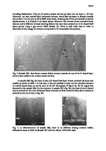
Er3+ Photoluminescence Properties of Erbium-doped Si/SiO2 Superlattices with sub-nm Thin Si Layers Yong Ho Ha1, Sehun Kim1, Dae Won Moon2, Ji-Hong Jhe3 and Jung H. Shin3 1 Department of Chemistry, School of Molecular Science, Korea Advanced Institute of Science and Technology (KAIST), 373-1 Kusung-dong, Yusung-Gu, Taejon, KOREA 2 Nano Surface Group, Korea Research Institute of Standards and Science (KRISS), Doryongdong 1, Taejon 305-606, KOREA 3 Department of Physics, Korea Advanced Institute of Science and Technology (KAIST), 373-1 Kusung-dong, Yusung-Gu, Taejon, KOREA. ABSTRACT The effect of varying the Si layer thickness on the Er3+ photoluminescence properties of Er-doped Si/SiO2 superlattice is investigated. We find that as the Si layer thickness is reduced from 3.6 nm down to a monolayer of Si, the Er3+ luminescence intensity increases by over an order of magnitude. Temperature dependence of the Er3+ luminescence intensity and timeresolved measurement of Er3+ luminescence intensity identify the increase in the excitation rate as the likely cause for such an increase, and underscore the importance of the Si/SiO2 interface in determining the Er3+ luminescence properties. INTRODUCTION Since the first work by Ennen [1], Er doping of silicon has received a great deal of attention as it promises the possibility of developing Si-based optoelectronics. However, despite some early success, it has been recognized that the small bandgap of bulk Si [2] and strong Er-carrier interaction [3,4] render practical application of Er-doped bulk Si difficult. However, such problems can be overcome by using Si nanostructures instead. In particular, unlike Er doping of Si nanoclusters, Er doping of Si/SiO2 offers the advantages of the possibility of direct control over the thickness of the layers and the location of Er, and consequently over the quantum effect and the Er-carrier interaction, respectively. Furthermore, such Si/SiO2 superlattice thin films are much more amenable to current transport. Previously, we have demonstrated that by confining Er atoms to the SiO2 layers and depositing nm-thin buffer layers of pure SiO2 between Si layers and Er-doped SiO2 layers, it is possible to suppress carriermediated de-excitation mechanisms to such a degree that several orders of magnitude enhancement in Er3+ luminescence intensity can be achieved [5,6]. In this paper, we investigate the effects of varying the Si layer thickness on the Er3+ photoluminescence (PL) properties of erbium-doped Si/SiO2 superlattices. We find that as the Si layer thickness is reduced from 3.6 nm down to a monolayer, Er3+ luminescence intensity increases by over an order of magnitude. The temperature dependence of the Er3+ luminescence intensity and timeresolved measurement of Er3+ luminescence intensity suggest the increase in the excitation rate as the likely cause for such an increase. The results underscore the importance of Si/SiO2 interface in determining the Er3+ luminescence, and suggest that for possible applications, the surface/volume ratio of Si regi
Data Loading...