Fabrication of 3.4kV high voltage n-type 4H-SiC Schottky barrier diodes using thick epitaxial layers
- PDF / 639,474 Bytes
- 9 Pages / 595 x 842 pts (A4) Page_size
- 82 Downloads / 356 Views
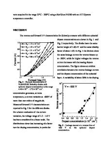
Fabrication of 3.4kV high voltage n-type 4H-SiC Schottky barrier diodes using thick epitaxial layers Takashi Tsuji, Hiroyuki Fujisawa, Shinji Ogino, Hidekazu Tsuchida1, Isaho Kamata1, Tamotsu Jikimoto1 and Kunikazu Izumi1 Fuji Electric Corporate Research and Development, Ltd., 2-2-1 Nagasaka, Yokosuka City, 240-0194 Japan 1 Central Research Institute of Electric Power Industry, 2-6-1 Nagasaka, Yokosuka City, 240-0196 Japan ABSTRACT Fabrication and evaluation of high voltage n-type 4H-SiC Schottky barrier diodes (SBDs) using 27µm thick epitaxial layers were presented. To achieve the ideal value of the breakdown voltage, various parameters of junction termination extension (JTE) were investigated. We concluded that the termination of triple rings with the concentrations of 6x10¹⁷, 3x10¹⁷, 1.5x1017cm-3 outwardly was best with the simulations. The SBDs with this termination showed the blocking voltage up to 3.4kV, which is almost the ideal value. We also investigated the distribution of leakage currents at -600V in SBDs with various diameters up to 4mm. High yield was obtained in the SBDs with the diameters below 2mm. The SBDs with high leakage currents showed the excess currents in the low forward voltage region and lots of bright spots could be observed by optical beam induced current analysis.
INTRODUCTION Recently, various kinds of devices of silicon carbide have been realized by the improvement of wafer quality[1], device processing and the new ideas which improve device performance. Especially, Schottky barrier diodes (SBDs) have been expected to replace Si pin diodes for several reasons[2][3]. First, SiC- SBDs show low switching loss because of the low reverse recovery currents, and the switching loss remain constant with the increase of temperature owing to the wide band gap of SiC. Second, SiC-SBDs could sustain high blocking voltage identical to Si pin diodes with thinner epitaxial layers, because the critical electric field of SiC is one order of magnitude higher than that of Si. Therefore, SiC-SBDs could reduce power dissipation compared to Si-pin diodes. One of the applications of SiC-SBDs is a power transmission system. Since it requires high blocking voltages more than several kV, the epitaxial layers with the thickness of more than a few 10µm are necessary. High growth rate has been desired to grow thick epitaxial layers. Epitaxial growth with high growth rate was realized by low pressure chemical vapor deposition (LPCVD) with the vertical hot wall reactor[4]. In this paper, we fabricate and evaluate high voltage n-type 4H-SiC SBDs using these thick epitaxial layers by a hot wall LPCVD system. H5.36.1
EXPERIMENTAL DETAILS The cross sectional structure of Schottky barrier diodes is shown in Figure 1. N-type 4H-SiC substrates were supplied by Cree Research Inc. The doping concentration of the substrates is more than 1018cm-3, the c axis tilts 8 degrees to (11 2 0) direction. The epitaxial layers were grown on (0001)Si face of the substrates by the hot-wall LPCVD system[4]. The thickness of these epitaxi
Data Loading...