Fabrication of GaN layer with Low Dislocation Density using Facet controlled ELO technique
- PDF / 891,562 Bytes
- 6 Pages / 612 x 792 pts (letter) Page_size
- 54 Downloads / 282 Views
Fabrication of GaN layer with Low Dislocation Density using Facet controlled ELO technique H. Miyake1, H. Mizutani1, K. Hiramatsu1, Y. Iyechika2, Y. Honda2 and T. Maeda2 1 2
Dept. of Electrical and Electronic Engineering, Mie University, Tsu, Mie 514-8507, Japan Tsukuba Research Laboratory, Sumitomo Chemical Co., Ltd, Tsukuba 300-3294, Japan
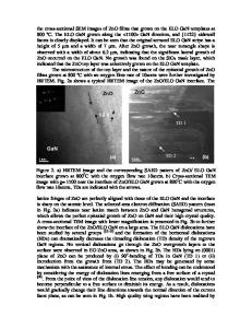
ABSTRACT GaN layers with low dislocation density have been fabricated be means of facet-controlled epitaxial lateral overgrowth (FACELO) via low-pressure metalorganic vapor phase epitaxy (LP-MOVPE). The distribution of the dislocations in FACELO GaN was inspected by observation of InGaN growth pits. For FACELO with {11-20} facets as the first step, the dislocations concentrate only in the window region. For FACELO with {11-22} facets as the first step, the dislocations exist only in the coalescence region. The double FACELO, which was FACELO with {11-20} on FACELO with {11-22}, was demonstrated and dislocation density of less than 105 cm-2 was achieved.
INTRODUCTION GaN and related nitride semiconductors have received much attention as one of the most attractive wide-band-gap semiconductors applicable to optical and electronic devices. Since there is no suitable substrate that matches with GaN, the epitaxial growth of GaN were mainly employed on sapphire substrate using the low-temperature buffer-layer technique [1]. Lattice mismatch between GaN and sapphire is 13.8 %. Although progress in growth techniques, GaN epilayers grown on sapphire with the low-temperature buffer layer have a large number of threading dislocations of the order of 108 - 1010 cm-2. Epitaxial lateral overgrowth (ELO) [2] with selective area growth (SAG) is a promising technique to obtain a high-quality epitaxial GaN layer with low threading dislocation density. Usui et al. applied the ELO technique to GaN by HVPE and achieved low dislocation density of the order of 107 cm-2 in the thick GaN [3]. They called this technique FIELO (Facet Initiated ELO). Sakai et al. are reported the dislocation bending caused by the facet places in ELO, so that the dislocation density is reduced [4]. Nam et al. are performed the ELO via MOVPE and achieved low dislocation density above the mask [5]. The ELO GaN layer has much contributed to improving device performance such as LDs with a long lifetime [6]. Recently, it was found that two-step ELO growth of GaN is a useful technique to improve crystalline quality of the ELO GaN through the facet control [7-10]. Hereafter, we call this technique “FACELO” (Facet Controlled ELO). It is based on the control of GaN structures by changing growth conditions during the ELO process [11]. In this paper, the typical two kinds of FACELO techniques of GaN were demonstrated via LP-MOVPE and the distribution of the dislocations was investigated. In order to reduce dislocation density further, double FACELO was employed.
G5.3.1
EXPERIMENTAL The ELO of GaN via a LP-MOVPE system using a horizontal reactor was performed on a 3–4 µm thick (0001) GaN layer which had been prepared on a (0001) s
Data Loading...