Flat-band Voltage Shift of MOS Capacitors with Tantalum Nitride Gate Electrodes Induced by Post Metallization Annealing
- PDF / 325,468 Bytes
- 6 Pages / 612 x 792 pts (letter) Page_size
- 80 Downloads / 267 Views
E6.27.1
Flat-band Voltage Shift of MOS Capacitors with Tantalum Nitride Gate Electrodes Induced by Post Metallization Annealing M. Kadoshima1, K. Yamamoto1, H. Fujiwara1, K. Akiyama1, K. Tominaga1, N. Yamagishi1, K. Iwamoto1, M. Ohno1, T. Yasuda2, T. Nabatame1 and A. Toriumi2,3 1 MIRAI, Association of Super-Advanced Technologies (ASET), AIST Tsukuba SCR Building, Tsukuba, 305-8569, Japan 2 MIRAI, Advanced Semiconductor Research Center (ASRC), AIST Tsukuba SCR Building, Tsukuba, 305-8569, Japan 3 Department of Materials Science, The University of Tokyo, 7-3-1 Hongo, Tokyo, 113-8656, JAPAN
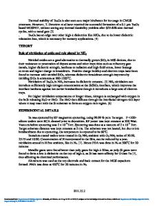
ABSTRACT We have investigated the flat-band voltage (VFB) shifts of tantalum nitride gate MOS capacitors prepared by two methods. One is CVD-tantalum nitride (CVD-TaN) deposited by the chemical vapor deposition technique using Ta[NC(CH3)2C2H5][N(CH3)2]3 as a precursor, and the other one is sputtered tantalum nitride (sp-TaN) electrodes deposited by reactive DC magnetron sputtering. In the case of the CVD-TaN electrodes, the effective work function estimated from the relationship between VFB and the equivalent oxide thickness (EOT) of the MOS capacitors was about 4.4eV after post metallization annealing (PMA) at 400ºC, and shifted to the mid-gap after PMA at 950ºC. Moreover, the VFB values of MOS capacitors with sp-TaN electrodes also showed the same behavior after PMA. This shift is mainly dependent on the PMA temperature, regardless of the deposition method used. Similar VFB shifts induced by PMA were also observed in sp-TaN/ Al2O3/ SiO2/ p-Si and sp-TaN/ TaOx/ SiO2/ p-Si capacitors. However, in the case of the sp-TaN/ TaOx/ SiO2/ p-Si capacitors, the VFB shift was also observed when the PDA temperature after the TaOx deposition was 800ºC and the PMA temperature after the TaN deposition was only 400ºC. These results strongly suggest that this VFB shift caused by the PMA originates from a thin interfacial oxide layer between the TaN gate electrode and the dielectrics. Therefore, the maximum processing temperature after gate electrode deposition is important in order to control the threshold voltage of tantalum nitride gate MOSFETs.
INTRODUCTION As metal-oxide-semiconductor (MOS) devices are scaled down in size, the required equivalent gate oxide thickness decreases to less than 2 nm. Alternative gate dielectrics such as high-k materials have been extensively studied [1]. On the other hand, poly-silicon gate electrodes are encountering problems with gate depletion and boron penetration. Metal gate electrodes are effective in overcoming these problems because metal electrodes do not deplete, unlike semiconductor electrodes such as doped poly-silicon, and do not ordinarily need doping. For these reasons, many kinds of metal gate electrodes have been studied [2-6]. Among the possible metal gate electrodes, TaN gate electrodes are reported to have high thermal stability [2, 3, 6]. However, reported values for the flat-band voltages (VFB) of MOS capacitors with TaN gate electrodes exhibit a broad distribution [2, 3, 6], presumably beca
Data Loading...