Grain Orientation and Strain Measurements in Sub-Micron wide Passivated Individual Aluminum Test Structures
- PDF / 1,205,541 Bytes
- 6 Pages / 612 x 792 pts (letter) Page_size
- 6 Downloads / 243 Views
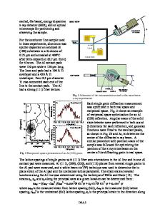
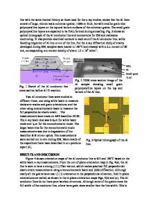
Grain Orientation and Strain Measurements in Sub-Micron wide Passivated Individual Aluminum Test Structures N. Tamura1, B. C. Valek2, R. Spolenak3, A. A. MacDowell1, R. S. Celestre1, H.A.Padmore1, W. L. Brown3, T. Marieb5, J. C. Bravman2, B. W. Batterman1 and J. R. Patel 1,4 1 ALS/LBNL, 1 Cyclotron Road, Berkeley CA 94720, USA 2 Dept. of Mat. Sci. & Eng., Stanford University, Stanford, CA 94305, USA 3 Bell Laboratories, Lucent Technologies, Murray Hill NJ 07974, USA 4 SSRL/SLAC, Stanford University, Stanford, CA 94309, USA 5 Intel Corp., Portland, OR 97124, USA ABSTRACT An X-ray microdiffraction dedicated beamline, combining white and monochromatic beam capabilities, has been built at the Advanced Light Source. The purpose of this beamline is to address the myriad problems in Materials Science and Physics that require submicron x-ray beams for structural characterization. Many such problems are found in the general area of thin films and nano-materials. For instance, the ability to characterize the orientation and strain state in individual grains of thin films allows us to measure structural changes at a very local level. These microstructural changes are influenced heavily by such parameters as deposition conditions and subsequent treatment. The accurate measurement of strain gradients at the micron and sub-micron level finds many applications ranging from the strain state under nano-indenters to gradients at crack tips. Undoubtedly many other applications will unfold in the future as we gain experience with the capabilities and limitations of this instrument. We have applied this technique to measure grain orientation and residual stress in single grains of pure Al interconnect lines and preliminary results on post-electromigration test experiments are presented. It is shown that measurements with this instrument can be used to resolve the complete stress tensor (6 components) in a submicron volume inside a single grain of Al under a passivation layer with an overall precision of about 20 MPa. The microstructure of passivated lines appears to be complex, with grains divided into identifiable subgrains and noticeable local variations of both tensile/compressive and shear stresses within single grains. INTRODUCTION The reliability of integrated circuits depends on the time to failure of the polycrystalline Al or Cu based lines used as device interconnections. Understanding interconnect failure mechanisms in order to predict and improve their lifetime is therefore a major concern in the semiconductor industry. Electromigration is the material transport resulting from the momentum transfer of the electron wind on the constitutive atoms under high current density. Damage by void formation, growth, and migration, ultimately causing open circuit failure, was very early identified as the main mechanism responsible for failure [1]. Voids form to overcome high stresses, which develop in the material during both fabrication and electromigration. The elevated residual stress, which builds up in the lines during the fabricatio
Data Loading...


