Growth and Characterization of Silicon-Germanium Films on Oxide by VLPCVD/PE-VLPCVD
- PDF / 1,317,696 Bytes
- 6 Pages / 414.72 x 648 pts Page_size
- 4 Downloads / 213 Views
ABSTRACT Results of Sil-.Ge_ deposition on oxide-coated Si substrates using a PE-VLPCVD (Plasma-Enhanced Very-Low-Pressure Chemical Vapor Deposition) reactor are presented. Thin layers of poly-Sil_,Ge, deposited with SiH 4 and GeH 4 at < 600*C had low C and O levels. Two growth modes were examined at 500'C: plasma-initiated thermal growth (VLPCVD) and full plasma-enhanced deposition (PE-VLPCVD). In both cases, Ge incorporation increases sublinearly with gas ratio, growth rates increase with Ge content, and the transition temperature between polycrystalline and amorphous deposition is lower for Sil_,Ge, than Si. On the other hand, compared to thermal growth, plasma-enhanced deposition promotes not only higher growth rates but also improved structural properties such as smoother surface morphology, more columnar and oriented grains, and the unique feature of direct deposition onto oxide.
INTRODUCTION Polycrystalline Si1_.Ge. (poly-Si,-Ge.) alloy materials are currently of interest for thin-film transistor (TFT) applications in integrated circuits and large area flat panel displays. Compared to poly-Si, poly-Sil-,Ge, offers lower temperatures for deposition and processing1 and potentially higher effective carrier mobilities, yet it remains compatible with existing Si processing and integrated circuit technologies. TFT applications include load devices for static random-access memory (SRAM) cells 2 and switching elements and integrated driver circuitry for flat-panel displays such as the active-matrix liquid crystal display (AMLCD).' The predominant techniques for growth of poly-Sil.,Ge, materials are by chemical vapor deposition (CVD). Conventional low-pressure CVD (LPCVD) has been used to grow poly-Sil_,Ge, as a variable work-function gate material in CMOS technology, 4 as the channel layer for PMOS transistors, 5 and as a material for low thermal budget CMOS TFT technology. 1 Poly-Sil_.Ge, has also been grown by rapid thermal CVD (RTCVD) as selective diffusion sources for ultra-shallow junctions in Si. 6 However, thermal CVD of SilxGe, has limitations such as higher oxygen contents1' 7 and difficulty nucleating on oxide"'9 both of which can inhibit optimal perfoimance in TFT devices. Our work addresses these issues utilizing a flexible very-low-pressure CVD (VLPCVD) system which has a low base pressure and the capability of plasma-enhanced -deposition. This work explores the growth of Sil.,Ge, on oxide using thermal VLPCVD and plasma-enhanced (PE-) VLPCVD. Results from characterization of these poly-Sii_,Ge, films will be discussed. 603 Mat. Res. Soc. Symp. Proc. Vol. 317. ©1994 Materials Research Society
C•10
E 10T
V~
TWO
~
0
Ir-Ls
20~
10
50
00
1500
20
eph(Angstroms)
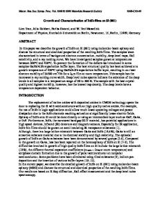
Figure 1: Cross-sectional schematic of the PEVLPCVD reactor chamber.
Figure 2: SIMS analysis of background C ,and 0 levels in a poly-Sii_=Gex film grown by PE-VLPCVD at 500°C.
EXPERIMENTAL PROCEDURE The research tool used for Sii_=Ge= growth, shown in Figure 1, is a flexible very-lowpressure chemical vapor deposition (VLPCVD) reactor
Data Loading...