Growth and Surface Reconstructions of AIN(0001) Films
- PDF / 412,026 Bytes
- 6 Pages / 612 x 792 pts (letter) Page_size
- 42 Downloads / 325 Views
Y3.5.1
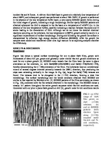
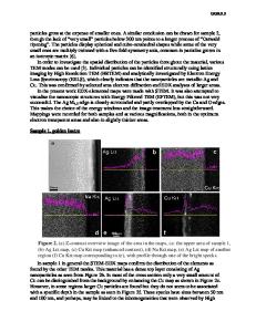
Growth and Surface Reconstructions of AlN(0001) Films C. D. Lee1*, Y. Dong1 , R. M. Feenstra1, J. E. Northrup2, J. Neugebauer3 1 Dept. Physics, Carnegie Mellon University, Pittsburgh, PA 15213 2 Palo Alto Research Center, 3333 Coyote Hill Road, Palo Alto, California 94304 3 University of Paderborn, Warburger Str. 100, 33098 Paderborn, Germany ABSTRACT The growth and surface reconstructions of AlN(0001) films were studied. For moderately Alrich surfaces, the 2×6 structure is commonly observed in reflection high energy electron diffraction. It is found that this pattern consists of 2√3×2√3-R30° and 5√3×5√3-R30° reconstructions according to scanning tunneling microscopy. Similar to the Ga-rich GaN(0001) surface, these structures are determined to contain 2−3 monolayers of excess Al terminating the surface. Based on first-principles theory the structures are believed to contain a laterally contracted Al layer. At higher Al coverage a thick, flat Al film is found to form on the surface. A high density of growth spirals (associated with threading dislocations having full or partial screw character) is found to be present on the surface, although this density decreases with increasing growth temperature. INTRODUCTION AlN has been considered as a useful material for high temperature and high power electronic devices and also optoelectronic device applications. Since the lattice constant of AlN is relatively closely matched to that of SiC (+0.9%), it has been used as a buffer layer for high power electronic devices. In contrast to recent progress in identifying surface structural arrangements on GaN [1], there is only limited knowledge currently on the surfaces structures of AlN. Several studies have previously reported the symmetry of AlN surface reconstructions as seen by reflection high energy electron diffraction (RHEED) [2-9]. RHEED patterns with symmetries of 1×1 and 2×2 are commonly reported, a 2×6 pattern is also commonly seen, and a sequence consisting of 1×3, 3×3, and 6×6 is reported by several groups. (For RHEED on a surface with hexagonal symmetry, a 1×3 pattern corresponds to a √3×√3-R30° symmetry.) Structural arrangements associated with these reconstructions have not been determined. In this work we report on scanning tunneling microscopy (STM), reflection high energy electron diffraction (RHEED) and low energy electron diffraction (LEED) measurements of reconstructions of the AlN(0001) surface. EXPERIMENTAL AlN films were grown by plasma-assisted molecular beam epitaxy (PAMBE) as previously described [10]. In order to minimize surface roughening due to the –2.5% lattice mismatch of AlN relative to GaN, a sequence containing ≈1 nm-thick AlN layers followed by ≈2 nm-thick Sidoped GaN layers was deposited. An undoped AlN layer with thickness of about 10 nm was then deposited on top. Somewhat flatter morphology was obtained in this case compared to direct deposition of AlN on GaN. A growth temperature of 750−800°C was generally used although on a few occasions we have occasionally used higher growth tempe
Data Loading...