Growth of cubic boron nitride films on tungsten carbide substrates by direct current jet plasma chemical vapor depositio
- PDF / 1,562,928 Bytes
- 5 Pages / 612 x 792 pts (letter) Page_size
- 4 Downloads / 335 Views
Cubic boron nitride (cBN) film was deposited on Co-containing WC substrates by dc jet plasma chemical vapor deposition from an Ar–N2–BF3–H2 gas system. The formation of cobalt nitrides was observed at interface, and the hindrance of Co on cBN growth was demonstrated. Growth temperature and etching treatment of the substrate before deposition influenced the cBN growth greatly. At 1050 °C, cBN films were obtained on etched substrates but not on unetched substrates. At 1090 °C, cBN films were not obtained even on etched substrates. At 960 °C, cBN films deposited even on unetched substrate but the films always peeled off after exposing to air. The film quality of cBN deposited at 960 °C is better than that deposited at 1050 °C.
I. INTRODUCTION
Cubic boron nitride (cBN) is an important material with outstanding mechanical and physical properties. The hardness of about 9000 kg mm−2 (Ref. 1) makes cBN a superhard material only second to diamond and hence a natural candidate for hard and protective coatings. cBN is more attractive than diamond for tooling application because it does not react with ferrous metals and has a high resistance to oxidation at temperatures as high as 1300 °C.1,2 Due to its wide band gap and good thermal conductivity, cBN has potential applications for hightemperature and high-power electronics. In addition, cBN can be doped both p- and n-type, whereas n-type doping is still a challenge for diamond.3–6 However, the cBN technology developed so far is far behind that of diamond. The growth of cBN films at low pressure involves energetic ion bombardment, which generates high compressive stress in the films during deposition. The stress generally causes the film to crack and peel off when the film thickness exceeds 100 nm, and it is very difficult to deposit thick cBN films over 1 m.7–9 The problem of poor adhesion impedes the widespread application of the cBN films. Because of the ion bombardment, the crystallinity of cBN films is very poor, and the crystal size is limited to a few to tens of nanometers, although small crystal size is useful for some applications such as to use smooth surfaces. The deposition of cBN films on Co-cemented tungsten carbide (WC-Co) is
a)
Address all correspondence to this author. e-mail: [email protected] DOI: 10.1557/JMR.2004.0188 1408
http://journals.cambridge.org
J. Mater. Res., Vol. 19, No. 5, May 2004 Downloaded: 21 Mar 2015
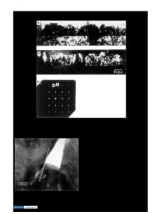
very seldom reported, whereas diamond-coated cutting tools are commercially available now. Recently, thick and highly crystallized cBN films were synthesized by bias-assisted dc plasma-jet chemical vapor deposition (CVD) from the Ar–N2–BF3–H2 gas system in our group.10 A film thickness of 27 m was achieved after growing for 180 min and faceted crystals with a size of 1 m were observed by scanning electron microscopy (SEM).11,12 The phase purity of cBN is generally more than 90%. A combined effect of the introducing of fluorine, low bias voltage, and high plasma density is responsible for this significant improvement. The t
Data Loading...