Hardness and Elastic Modulus Measurements in CdTe and ZnTe Thin Film and Bulk Samples and ZnTe-CdTe Superlattices
- PDF / 346,261 Bytes
- 6 Pages / 420.48 x 639 pts Page_size
- 27 Downloads / 356 Views
HARDNESS AND ELASTIC MODULUS MEASUREMENTS IN CdTe AND ZnTe THIN FILM AND BULK SAMPLES AND ZnTe-CdTe SUPERLATTICES L. J. Farthing*, T. P. Weihs*, D. W. Kisker**, J. J. Krajewski**, M. F. Tang*, and D. A. Stevenson* * Department of Materials Science, Stanford University, Stanford, California 94305 ** AT&T Bell Laboratories, Homdel, New Jersey 07733
ABSTRACT Hardness and modulus values of bulk and epilayer ZnTe and CdTe samples and of ZnTe-CdTe superlattices are reported. Both hardness and Young's modulus values increase with increasing ZnTe content in the ZnCdTe samples. Alloying effects and strains in the superlattice structure are proposed to explain the strengthening.
INTRODUCTION Compound semiconductor superlattices are of interest to the materials community because bandgaps can be finely tuned by the proper choice of the semiconductor materials and layer thicknesses. Mechanical properties relate to the changes in electronic and optical properties that may accompany the processing of semiconductor materials into devices, particularly the introduction of dislocations upon thermal processing and the application of films. Furthermore, the mechanical properties are of concern in the integrity of devices during service. In this paper, we report hardness and elastic modulus values for ZnTe and CdTe epilayer and bulk samples and ZnTeCdTe strained layer superlattices. The ZnTe-CdTe system is of interest because of its promising optical properties [1].
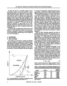
EXPERIMENTAL The samples consist of two sets of ZnTe-CdTe strained layer superlattices grown by atmospheric pressure organometallic vapor phase epitaxy (OMVPE) [1], and epilayer and bulk samples of ZnTe and CdTe. The first set of the superlattices consists of 200 cycles of 25 A ZnTe and 50 A CdTe with a 25 A CdTe cap and a 1.0 gim ZnTe buffer layer on a (100) GaAs substrate. The other set of superlattice samples consists of 200 cycles of 25 A CdTe and 50 A ZnTe with a 25 A CdTe cap and a 1.0 gim ZnTe buffer layer on a (100) GaAs substrate. The ZnTe and CdTe have a lattice mismatch of 6%, so these are strained layer superlattices. The (100) ZnTe epilayer and (100) CdTe epilayer are grown on (100) GaAs substrates by OMVPE for thicknesses of 2.0 gIm. The bulk samples are a single crystal (100) CdTe sample and a coarse grained ZnTe sample. X-ray diffraction measurements were made using a Picker diffractometer with a Cu Kc source. Hardnesses were measured by a Vickers hardness tester and a Nanoindenter, which can measure the hardness of very thin films. Important parameters of the Nanoindenter are a displacement resolution of 2 A and a force resolution of 0.5 mN [21. The data from the Nanoindenter give hardness values as a function of plastic Mat.Res. Soc. Symp. Proc. Voi. 130. r199 Materials Resarch Socity
124
depth, while Young's modulus values can be calculated from the unloading portion of the load versus depth indentation curves. Most samples were tested for depths between 20 and 1500 nm; however, for the purpose of analysis, only the indentations with depths between
Data Loading...