Heterostructure for UV LEDs Based on Thick AlGaN Layers
- PDF / 101,967 Bytes
- 4 Pages / 612 x 792 pts (letter) Page_size
- 20 Downloads / 385 Views
Internet Journal Nitride Semiconductor Research
Heterostructure for UV LEDs Based on Thick AlGaN Layers A. V. Sakharov1, W. V. Lundin1, A. Usikov1, U. I. Ushakov1, Yu A. Kudriavtsev1, A.V. Lunev1, Y.M. Sherniakov1 and N.N. Ledentsov1 1Ioffe
Physical-Technical Institute,
(Received Monday, June 22, 1998; accepted Friday, September 25, 1998)
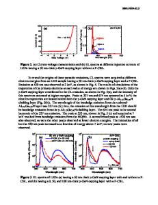
Thick AlGaN layers and GaN/AlGaN heterostructures were grown by low pressure MOCVD on (0001) sapphire substrates utilizing a low temperature AlGaN buffer layer. The distribution of Al in the thick AlGaN layers was observed to be non-uniform as a function of depth. The Al content gradually increases from the substrate towards the epilayer surface. Moreover, fluctuations of Al content are also noticeable. The saturation of impurity-related emission with increasing current density was observed in EL spectra of LEDs consisting of AlGaN/GaN/AlGaN DH sandwiched by a 2 µm-thick bottom layer of GaN:Si and 0.5 µm-thick layer of GaN:Mg. The dominant near-band edge emission of the GaN active layer was found to be strongly absorbed in the thick bottom layer. Utilizing a 2 µm-thick AlGaN bottom layer instead of the GaN one allowed the absorption edge to be shifted towards higher energies. A single peak at 362 nm with FWHM of 14 nm was observed in this type of LED. Luminescence properties of various types of heterostructures are also discussed.
1
Introduction
In recent years, remarkable progress in the technology of bright blue-green AlGaInN light emitting diodes (LEDs) and laser diodes has been achieved [1] [2]. The active region of these LEDs with either single- or multiple-quantum well structure are created from doped and undoped InGaN films. The visible emission from that active region does not absorb in GaN layers that promote the high-efficiency LED fabrication. However, ultra-violet (UV) LEDs are also of interest because of their potential use in white light conversion utilizing luminescent solid, in optical analysis of organic molecules, drug testing and other medical applications [3] [4]. Further advancement toward the ultraviolet spectral range can be accomplished by utilizing near-band-edge emission of GaN active layer in GaN-AlGaN heterostructures. But there is a strong absorption of the emission in a passive GaN region of the structure resulting in shifting of the peak emission to the long wavelength region. The aim of this work is to minimize the absorption of the near-band-edge emission and to fabricate UV LEDs based on thick AlGaN layers. 2
Experiment
The AlGaN layers and GaN/AlGaN double heterostructures (DH) were grown by MOCVD in a horizontal
reactor with an RF heated graphite susceptor at a low pressure of 200 mbar. Ammonia, trimethylgallium (TMG) and trimethylaluminum (TMA) were applied as component precursors. Purified hydrogen was used as a carrier gas. Silane and biscyclopentadienyl magnesium were used for doping. The substrates were (0001) optical grade polished sapphire. The growth procedure involved the buffer GaN layer growth at a low temperature (520 °C) f
Data Loading...


