High pressure annealing of HVPE GaN free-standing films: redistribution of defects and stress
- PDF / 273,600 Bytes
- 6 Pages / 612 x 792 pts (letter) Page_size
- 103 Downloads / 250 Views
E8.18.1
High pressure annealing of HVPE GaN free-standing films: redistribution of defects and stress T. Paskova1, T. Suski2, M. Bockowski2, P.P. Paskov1, V. Darakchieva1, B. Monemar1, F. Tuomisto3, K. Saarinen3, N. Ashkenov4, M. Schubert4, C. Roder5 and D. Hommel5 1 Department of Physics and Measurement Technology, Linköping University, S-581 83 Linköping, Sweden 2 High Pressure Research Center, Unipress, Polish Academy of Sciences, 01-142 Warsaw, Poland 3 Helsinki University of Technology, P.O. Box 1100, 02015 HUT, Finland 4 Fakultät für Physik and Geowissenschaften, Universität Leipzig, 04103 Leipzig, Germany 5 University of Bremen, Institute of Solid State Physics, 28359 Bremen, Germany
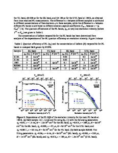
ABSTRACT The effect of high temperature, high pressure annealing on morphology, optical and structural properties of free-standing GaN films grown by hydride vapor phase epitaxy is studied. The annealing is found to change the intensities of the photoluminescence peaks as a result of a redistribution of the impurities and native defects in the thick GaN films. A positron annihilation study shows a decrease of the Ga vacancy-related defects below the detection limit after the annealing. The defect redistribution is correlated with a flattening of the stress distribution across the thickness, as revealed by micro Raman study, and with a decrease of the curvature of the annealed free-standing films.
INTRODUCTION Over the last few years, considerable progress has been made in the development of hydride vapor phase epitaxy (HVPE) growth of thick GaN layers. Free-standing HVPE-GaN films are currently considered as the most promising substitute for the native bulk nitride substrate, because of the difficulties in the growth of bulk GaN. Free-standing GaN wafers have been demonstrated by several groups and are even commercially available recently. However, a critical remaining question is the high and non-uniform distribution of dislocations [1-3], impurities [4-6], native defects [7], and stress [8-11] across the thickness, as well as wafer bending [12,13] and cracking [14,15]. The latter prevents the reproducible growth of large-area GaN substrates, and thus a proper understanding of the reasons for that is of crucial importance. The high-temperature annealing as an important tool in the material research is expected to lead to redistribution of the defects and consequently to a change of electrical, optical and structural parameters of the material. In addition, a study of the change of the defect content and distribution under the annealing treatment can provide useful insight into the defects responsible for sample bending. In this work we study the defect redistribution in free-standing HVPE-GaN layers caused by high temperature (HT) high pressure (HP) annealing, and its impact on residual stress and bending of the thick free-standing GaN films.
E8.18.2
EXPERIMENTAL DETAILS The HVPE-GaN films were grown on a metalorganic vapor phase epitaxial GaN template supplied by Lumilog, France. The template with 3-nm-thick SiN mask stri
Data Loading...