High quality GaN layers grown on slightly miscut sapphire wafers
- PDF / 1,856,883 Bytes
- 6 Pages / 612 x 792 pts (letter) Page_size
- 12 Downloads / 384 Views
0892-FF21-04.1
High quality GaN layers grown on slightly miscut sapphire wafers P. Brückner1, M. Feneberg2, K. Thonke2, F. Habel3, F. Scholz1 Optoelectronics Department, Ulm University, 89081 Ulm, Germany 2 Semiconductor Physics Department, Ulm University, 89081 Ulm, Germany 3 Freiberger Compound Materials GmbH, 09599 Freiberg, Germany 1
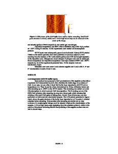
ABSTRACT HVPE grown layers typically show a high density of pyramidal structures on the surface. We found that a slight off-orientation of the substrate totally suppresses the development of these structures. Further we found that a misorientation towards the m-plane of GaN features a smoother surface morphology as compared to an off-orientation towards the a-plane. After the improvement of the surface morphology and other properties of the HVPE grown layers, we studied self-separation processes. Our approaches to remove the thick GaN layer from the substrate were the introduction of a low-temperature intermediate layer and a structured dielectric mask.
INTRODUCTION The improvement of GaN based electronic and optoelectronic devices, especially for short wavelength optoelectronics, is still limited by the fact that the epitaxial structures have to be grown on substrates like sapphire or SiC, because high quality bulk GaN wafers are still not readily available. The growth on foreign substrates causes a high defect density, which limits the efficiencies and life times of these devices. Therefore, the heteroepitaxial growth by hydride vapour phase epitaxy (HVPE) of thick GaN layers which can be used as quasi-substrates for the device epitaxy has been developed by several groups [1,2]. On such layers, excellent electronic and optoelectronic devices, in particular laser diodes [3] and light emitting diodes [4] have been fabricated. HVPE grown layers, however, still suffer from several problems. They normally show a quite rough pyramidally shaped surface, thus requiring a polishing step before their use in a following device growth. To reduce the strain of those layers and the bowing, it is necessary to remove the foreign substrate after the HVPE process to get free-standing GaN wafers. We studied the influence of several growth parameters on the electrical and optical properties and the surface morphology of the HVPE grown layers. Quite recently, several groups have reported that a slight substrate misorientation may improve the GaN layer quality considerably in MOVPE [5, 6]. Our own preliminary experiments showed that the misorientation of the wafer is of major importance also in HVPE [7, 8]. Hence, we have systematically investigated the influence of the substrate miscut on the HVPE grown layer properties by varying angle and direction of the misorientation of the sapphire substrate used. For a further improvement of GaN-based devices it is necessary to remove the foreign substrate from the HVPE-grown layer. Several groups developed such a process. One possibility is to remove the foreign substrate by laser lift-off (LLO) [9] or by using GaAs as substrate for the HVPE growth, which c
Data Loading...