High-resolution transmission electron microscopy (HRTEM) observation of dislocation structures in AlN thin films
- PDF / 1,081,500 Bytes
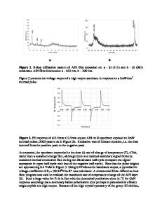
- 7 Pages / 612 x 792 pts (letter) Page_size
- 84 Downloads / 423 Views
Naoya Shibata Institute of Engineering Innovation, School of Engineering, The University of Tokyo, Bunkyo, Tokyo 113-8656, Japan; and PRESTO, JST, Kawaguchi, Saitama 332-0012, Japan
Teruyasu Mizoguchi and Masakazu Sugiyama Institute of Engineering Innovation, School of Engineering, The University of Tokyo, Bunkyo, Tokyo 113-8656, Japan
Yukihiro Shimogaki and Jung-Seung Yang Department of Materials Engineering, School of Engineering, The University of Tokyo, Bunkyo, Tokyo 113-8656, Japan
Takahisa Yamamoto Department of Advanced Materials Science, Graduate School of Frontier Science, The University of Tokyo, Kashiwa, Chiba 277-8651, Japan
Yuichi Ikuharaa) Institute of Engineering Innovation, School of Engineering, The University of Tokyo, Bunkyo, Tokyo 113-8656, Japan; and WPI Advanced Institute for Materials Research, Tohoku University, Sendai 980-8577, Japan (Received 28 December 2007; accepted 5 May 2008)
The structure and configuration of threading dislocations (TDs) in AlN films grown on (0001) sapphire by metal–organic vapor phase epitaxy (MOVPE) were characterized by high-resolution transmission electron microscopy (HRTEM). It was found that the TDs formed in the films were mainly the perfect edge dislocations with the Burgers vector of b ⳱ 1⁄3〈112¯0〉. The majority of the edge TDs were not randomly formed but densely arranged in lines. The arrays of the edge TDs were mainly observed on the {112¯0} and {101¯0} planes. These two planes showed different configurations of TDs. TD arrays on both of these planes constituted low-angle boundaries. We suggest that these TDs are introduced to compensate for slight misorientations between the subgrains during the film growth.
I. INTRODUCTION
Group III nitrides such as AlN, GaN, InN, and their alloys have attracted much attention because of their potential applications for novel, high-performance electronic and optoelectronic devices. For the growth of group III nitride films, several thin-film techniques have been used, and sapphire (␣-Al2O3) has been generally used as a substrate. However, because of the large lattice mismatches between the films and the substrate, the films inevitably contain a high density of threading dislocations (TDs).1–8 These TDs are known to have detrimental
a)
Address all correspondence to this author. e-mail: [email protected] DOI: 10.1557/JMR.2008.0265 2188
http://journals.cambridge.org
J. Mater. Res., Vol. 23, No. 8, Aug 2008 Downloaded: 14 Mar 2015
effects on the properties of the films. For example, they sometimes behave as nonradiative recombination centers9–11 or charged scattering centers for carrier mobility.12,13 To obtain better property films, it is essential to understand the mechanism of the TD generation. So far, a number of studies concerning the formation mechanism of TDs have been reported. It has been suggested that the origin of TDs in group III nitride on sapphire is closely related to the peculiar growth mode, which is called “mosaic growth.”5–8,14 In large lattice-mismatched systems, film growth by
Data Loading...