I-V CHARACTERISTICS OF a-Si:H p-i-n Diodes with Uniform and Non-Uniform Defect Distributions
- PDF / 626,151 Bytes
- 6 Pages / 612 x 792 pts (letter) Page_size
- 80 Downloads / 335 Views
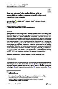
I-V CHARACTERISTICS OF a-Si:H p-i-n DIODES WITH UNIFORM AND NON-UNIFORM DEFECT DISTRIBUTIONS M.A. Kroon, R.A.C.M.M. van Swaaij, and J.W. Metselaar Delft University of Technology, Lab. of Electronic Components, Technology and Materials – DIMES, P.O. Box 5053, 2600 GB DELFT, the Netherlands ABSTRACT This paper compares a-Si:H p-i-n diodes having a spatially uniform distribution of defect states with diodes in which the defect distribution is non-uniform, i.e. equilibrated according to the Defect-Pool model. Diodes with a uniform defect distribution exhibit a clear dependence of the current-voltage characteristics on the width of the intrinsic region, whereas in equilibrated diodes, this dependence is absent. This difference is explained by comparing the space-charge distribution and the recombination profile of the intrinsic region in both types of diodes. INTRODUCTION Amorphous silicon (a-Si:H) p-i-n diodes are widely used as solar cells and as light sensing devices. An important and relatively easy method to characterize these devices is by currentvoltage (I-V) measurements. The forward current in a-Si:H diodes has been analyzed extensively in literature. Several conduction mechanisms have been proposed, like diffusion through the intrinsic region and tunneling at the interfaces [1,2]; at present, however, it is generally accepted that the forward current is driven by bulk recombination processes in the intrinsic region of the p-i-n diode [3,4]. An accurate description of the recombination processes in the a-Si:H p-i-n diode is complicated, since the recombination rate depends on the position in the intrinsic region. The main reason for this is the non-uniform defect distribution in the device caused by the equilibration of defects in a-Si:H, as described by the Defect-Pool Model (DPM) [5]. This model predicts a higher defect density near the p-i and i-n interfaces than in the center of the intrinsic region. The non-uniformity of the defect distribution is usually not taken into account in the models that are used to describe the dark I-V characteristics of a-Si:H p-i-n diodes [2,3,6]. In this paper, we present lateral a-Si:H p-i-n diodes which do have a spatially uniform distribution of defects in the intrinsic region (Fig. 1). These samples were made by depositing an intrinsic layer on an insulating substrate, which has a uniform defect density. Then the doped regions are formed by ion implantation at Figure 1. Schematic lay-out of the lateral room temperature. Within the experimental time a-Si:H p-i-n diode. frame the energetic density-of-states does not re-
A10.3.1
equilibrate at the modified position of the Fermi level. The defect states in the intrinsic region can be equilibrated by an additional anneal above the equilibration temperature of a-Si:H. Notice that in the doped regions the defect density is increased by the implantation damage, but these states do not contribute to the recombination in the device. The spatial distribution of defects influences the position and the shape of the recombination prof
Data Loading...