In Situ Design of Experiments for A Reactive Ion Etching Process
- PDF / 390,016 Bytes
- 6 Pages / 420.48 x 639 pts Page_size
- 82 Downloads / 295 Views
Abstract We introduce a new procedure to perform a design of experiments (DOE) for plasma etching processes. In particular, we use in situ etch rate estimations to maximize the number of observable setpoints during a single run of the etching process. This procedure is applied to characterize the spatial uniformity of a plasma chamber used in the manufacturing of flat panel displays.
1
INTRODUCTION
The industrial community widely accepts that the development of a new process is both costly and time consuming. This is largely due to the high number of experiments performed during a typical design of experiments (DOE) to accurately quantifies the relationship between the process input parameters and the product variables. In particular in semiconductor manufacturing, the standard DOE procedure is to characterize a single combination of input parameters (gas flow rates, RF power, pressure, etc.) per process run. In this case, the inputs remain fixed at a single operating condition, or setpoint, during the entire run. After the run has ended, the wafer parameters are obtained through ex situ measurement techniques. For example, an engineer developing a reactive ion etching (RIE) process expends precious time and money etching a number of wafers for the differ-
ent operating conditions necessary to obtain an accurate process characterization. As the price of a single wafer increases, test-wafer cost becomes more acute. Our concept of an in situ DOE maximizes the number of setpoints one can observe during a single etch by monitoring product variables in real-time during the run. We can substantially decrease the number of runs required for a complete characterization of the process. Therefore, the effective number of wafers and development time required to model a new process is reduced. Recently, there has been an increasing interest in the research community in obtaining in situ measurements techniques for semiconductor manufacturing processes [1, 2, 3, 4, 5, 6]. The in situ DOE strategy proposed in this paper is one more application that will strongly benefit from further results in this area. We apply the results of this research to the characterization of the etch rate uniformity across an RIE chamber used for manufacturing flat panel displays. One challenge in
165 Mat. Res. Soc. Symp. Proc. Vol. 569 ©1999 Materials Research Society
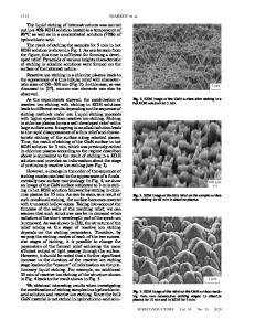
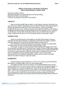
manufacturing flat panel displays is to reproduce the quality of the individual electronic devices across the plate. In that sense, etch rate uniformity across the plate is a critical parameter for the overall quality of the manufacturing process.
2
THE PRINCIPLE OF IN SITU DESIGN OF EXPERIMENTS
The mapping between process inputs and wafer parameters is generally quantified by the response surface of the process, which is commonly obtain after a design of experiments (DOE). This is a statistical technique that samples the input parameter space in order to obtain an accurate characterization of the process. The specific methodology for choosing the set of operating conditions is
Data Loading...