Influence of Preparation Conditions on Charge Carrier Dynamics in a-Si:H Determined by an In-Situ Technique
- PDF / 2,088,788 Bytes
- 6 Pages / 417.6 x 639 pts Page_size
- 44 Downloads / 284 Views
INFLUENCE OF PREPARATION CONDITIONS ON CHARGE CARRIER DYNAMICS IN a-Si:H DETERMINED BY AN iN-SIJU TECHNIQUE A. WERNER AND M. KUNST Hahn-Meitner-institut fUr Kernforschung Berlin, Bereich Strahlenchemie, G'ienicker Str. 100, D-1000 Berlin 39, Federal Reoublic of Germany ABSTRACT Contactless photoconductivity measurements with the time-resolved microwave conductivity technique have been performed during the growth of hydrogenated amorphous silicon films. it has been shown that low substrate temoerature and thin films lead to a larger electron decay rate and to an increased infrared absorption compared with high quality films. Addition of H2S to S4H 4 during the glow discharge orocess leads to a worse fi1m quality which can be detected in-situ. 1.
TNTROOUCTION
The preparation conditions of hydrogenated amorphous silicon in the glow-discharge process influence strongly the performance of optoelectronic devices made from this material. The spin density [If, as measured by the defect density, the absorption coefficient ¶2] are influenced by the production process and are normally measured after the preparation of the samples. efficient quality control, however, it is important to monitor For in-situ, i.e. during the oroduction orocess of the films, a physical property which reflects the defect density of the prepared samples. For pracbe contactless tical reasons in-situ measurements should preferably and ;or e'xampne optical ref'ectivity [3] or Photoinduced absorption TA measurements can be applied. In the oresent work the contactless time-resolved microwave conductivity (TRMC) technique '57 has been applied to analyze charge carrier dynamics in-situ in order to correlate the signals with the quality of the films produced. Time-resolved photoconductivity measurements should provide conclusions about the structure of this material, where the signal amplitude is related to the absorption coefficient and the decay time monitors the defect density. The TRMC-technique is based on the proportionality between the relative change of reflected microwave power and the induced photoconductivity [5]. The contribution of holes to the TRMC-signals can be neglected because the hole mobility is at least one order of magnitude smaller than the electron mobility [6]. 2. EXPERIMENTAL The a-Si:H films have been produced in a glow-discharge system by decomposing pure silane as described elsewhere [7]. The excess charge carriers have been induced by a Nd:YAG laser supplying pulses of 1064 nm and 532 with 15 ns pulse width (FWHM). The TRMC-measurements have been performed in a Ka band system (26.5 - 40 GHz) connected to the glow discharge
Mat. Res. Soc. Symp. Proc. Vol. 70. '1986 Materials Research Society
138
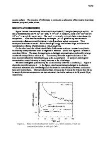
system. To avoid light interference effectsthe glass substrates were roughened. The experimental set-up is shown in fig. 1. The microwave system is connected via a glass window to the glow discharge chamber. A circulator separates the incident microwaves from the reflected ones which are transferred to a digitizer and a microcomput
Data Loading...