Infrared Optical Properties of Ion Implanted and Laser Annealed Silicon
- PDF / 711,251 Bytes
- 6 Pages / 414 x 635.4 pts Page_size
- 69 Downloads / 379 Views
Hess,
and Sigmon,
eds.
Laser and Electrcr-Becac Solid interactions and ::aterials Processing
163
INFRARED OPTICAL PROPERTIES OF ION IMPLANTED AND LASER ANNEALED SILICON
MASANOBU MIYAO, TERUAKI MOTOOKA, NOBUYOSHI NATSUAKI AND TAKASHI TOKUYAMA Central Research Laboratory, Hitachi Ltd., Kokubunji, Tokyo 185, Japan
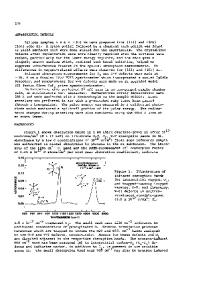
ABSTRACT Electronic states of extremely heavily doped n-type Si obtained by high dose ion implantation and laser annealing are investigated by measuring the infrared optical properties. Free carrier effective mass (m*) and carrier relaxation time (-) are obtained as 3 Values a function of carrier concentration (1019 - 5xlO1 cm- ). of m* and T increase and decrease, respectively, with the increase of carrier concentration. These results are discussed in relation to the occupation of electrons in a new valley of the conduction band.
INTRODUCTION Most deSilicon is the basic material of the modern electronics industry. vices have used Si crystals deliberately doped with impurities. The maximum 20 3 2 1 3 doping levels conventionally obtained have been 4x10 cm- , 2x10 cmand 21 3 2x10 cmfor B, As and P impurities respectively. This is because, these levels are limited by thermal equilibrium solid solubilityI. 2 Recently, new doping technique, ion implantation and laser annealing , has been developed. This has made it possible to dope Si with electrically active impurities significantly in excess of the thermal equilibrium3 solid solubility.4 Employing this technique, the resistivities of source, drain and gate regions 5 of MOS FET's or emitter regions of bipolar Trs have been reduced. This has contributed to the higher integration or faster operation of devices. However, the physical properties, especially electronic states, of extremely heavily doped Si layer have yet to be fully understood. Such clarification is necessary for precise analysis of device operation. This paper describes the infrared optical reflectance and transmittance of ion implanted and laser annealed Si layer, since these optical properties reflect the conduction band 6 structure . As a result, a new relation between free carrier effective mass and carrier concentration is established.
EXPERIMENTS Several p-type (100) Si wafers with 10 ohm-cm resistivities were implanted 16 2 14 cm- . This was to 5x10 by P (50 keV) or As (80 keV) ions at doses of 6x10 followed by Q-switched pulse ruby laser annealing (laser wavelength = 0.6943 pm, 2 pulse duration time = 25 ns, energy density = 0.5 -1.5 J/cm ). Carrier concentration profiles were determined by a combination of Hall effect measurement and conventional anodic oxidation layer removal method. Optical reflection and transmission were measured using a DIGILAB FTS-20 spectrom1 eter in the spectral region of 400 to 12000 cmat 300 K.
164
_ l was fulfilled for all samples. Thus, the validity of the method to obtain m* from optical reflectivity was proven. In the figure, m* values (0) derived from Fig. 3 are compared with that (o) obtained from Fig. 2. The same relation between m* and N was o
Data Loading...