Structural Defects in Laser Annealed Arsenic Implanted Silicon
- PDF / 1,404,691 Bytes
- 6 Pages / 420.48 x 639 pts Page_size
- 88 Downloads / 410 Views
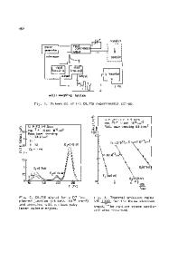
STRUCTURAL DEFECTS IN LASER ANNEALED ARSENIC IMPLANTE)D SILICON J. M. TONNERRE, M. MATSUURA* and G. S. CARGILL III IBM Research Division, T. J. Watson Research Center, Yorktown Ileights, NY 10598
L. W. HOBBS MIT, Dept. of Materials Science and Engineering, Cambridge, MA 02139
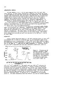
ABSTRACT Laser annealed arsenic implanted silicon specimens with doses ranging from 6xW015 to 7x11016 2 As/cm have been investigated by transmission electron microscopy (TEM) and double crystal xray diffractometry (DCD). For the highest implant dose, laser powers ranging from I.I to 2.2 2 J/cm have been used. Experimental observations show two new features for this kind of specimen. First, in some cases, TEM micrographs evidence small (-50A diameter) precipitate-like defects and/or dislocation loops confined within the heavily doped region. Second, in some cases, DCD shows a positive strain in addition to the negative strain attributed to 90% As in substitutional sites. X-ray rocking-curve simulations reveal that the negative strain drops to zero around IOO0A before the end of the As distribution. This might be related to the presence of Si interstitials in the deepest region of the As distribution. INTRODUCTION The controlled doping of semiconductors by selected impurities is of scientific and technological interest. It is well established that laser annealing processing can incorporate ion-implanted group Ill, V and VI elements as electrically active, substitutional impurities in silicon, at concentrations that far exceed equilibrium solubility limits [1,2]. Nevertheless, the electrical behavior of the more commonly used As in Si is not completely understood. Particularly, recent studies have focussed on the structural nature of electrically inactive As, when laser annealed As implanted specimens have undergone subsequent thermal annealing [3-6]. In this paper, we present RBS, TEM and DCD results with the goal of better understanding the influence of different preparation parameters (dose, laser power) on Si:As specimens prior to further annealing. Our results show that particular attention must be given to the influence of the laser power, and our results reveal two new features for the as-laser annealed samples. EXPERIMENTAL RESULTS Implantations of As were performed 7' off-axis in (100) Si wafers (Czochralski-grown, boron-doped, 10-20 £2-cm, 0.4 mm thick), at 100 keV and room temperature. The doses were in 15 2 the range from 6x10 to 7x10t6 As/cm . Laser annealing was carried out using a frequency-doubled Nd:YAG Q-switched laser. l)ifferent defocused beam sizes, near 50 Pim diameter, were used, 2 leading to surface energy densities of 1.1, 1.4, 1.9 and 2.2 J/cm . The sample was scanned with a 2 raster of overlapping pulses. Samples laser annealed with 1.1 and 1.4 J/cm did not recrystallize 2 epitaxially, in contrast to epitaxial recrystallization observed for 1.9 and 2.2 J/cm laser annealed samples. The homogeneity of the implanted layers and the laser annealed layers has been checked by measuring the electrical resistivity on different
Data Loading...