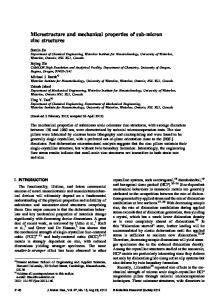
Mechanical Properties of 0.1 Micron Thick Simox Film Measured Using on-Chip Tensile Test System
- PDF / 486,744 Bytes
- 6 Pages / 612 x 792 pts (letter) Page_size
- 7 Downloads / 347 Views
MECHANICAL PROPERTIES OF 0.1 MICRON THICK SIMOX FILM MEASURED USING ON-CHIP TENSILE TEST SYSTEM J. Amano, T. Ando, M. Shikida, K. Sato and T. Tsuchiya* Dept. of Microsystem Engineering, Nagoya Univ., Furoh-cho, Chikusa, Nagoya 464-8603, Japan * Toyota Central R&D Labs Inc., Nagakute, Aichi 480-1192, Japan ABSTRACT We evaluated the mechanical properties of a very thin single-crystal-silicon film 140 nm thick fabricated from a SIMOX wafer using an on-chip tensile testing method. The silicon specimen oriented in the direction was integrated with a loading mechanism on the same chip, which was fabricated in three etching steps. The strain in the film was measured using a newly developed tensile testing system having a two-field-of-view microscope that allowed us to observe the elongation of the specimen directly. The measured fracture strain was distributed in the range of 2.4–3.2%, which is narrower than the range of 1.3–3.5% for a thicker 5-µm film. INTRODUCTION Characterization of the mechanical properties of thin films is necessary in order to design MEMS devices and predict the mechanical load limit, which enables one to discuss the reliability of the devices. For films whose thickness is on the nanometer order, we cannot ignore grain boundary and surface structures when considering the mechanical strength. In the case of brittle materials such as the silicon and silicon compounds generally used in MEMS devices, fractures are caused by defects existing in the crystal and on the surface. When the dimensions of the material become smaller, the material is regarded as being perfect without any defects, so its mechanical strength approaches the ideal value. Tensile tests for silicon film such as single-crystal-silicon and polysilicon have been carried out [1-3] and the size effect of the specimen was investigated. Characterization of the mechanical properties for nano-scale silicon film was done using a bending test [4]. The mean bending strength of nano-scale silicon film was reported to be 17.5 GPa, which is much larger than for microscale specimens. In this paper, we report on the fracture properties of nanometer-scale single-crystal-silicon film and compare them with those of thicker films. In order to fabricate the thin-film specimen, we used a SIMOX wafer having a 160-nm-thick silicon layer. We also evaluated a 140-nm-thick silicon specimen. The measured fracture strain was distributed in a narrower range than that of thicker films. EXPERIMENTAL PROCEDURE Single-crystal-silicon thin films as thin as 140 nm were obtained from a SIMOX (Sparation by IMplanted OXygen) wafer, which is a kind of SOI wafer. The 140-nm-thick silicon specimen B8.3.1
Figure 1. Single crystal silicon specimen fabricated from SIMOX wafer.
Figure 2. Testing device having silicon specimen and loading system.
Figure 3. Schematic view of cross-section of testing device during loading. fabricated for the tensile tests is shown in Figure 1. It is 140 µm long and 50 µm wide at the straight portion, and has stress relaxation zones at both ends.
Data Loading...