Microstructures of Si(111) on Ion Sputtering and Electron Annealing
- PDF / 4,324,323 Bytes
- 6 Pages / 420.48 x 639 pts Page_size
- 52 Downloads / 404 Views
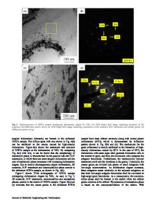
MICROSTRUCTURES OF Si(111) ON ION SPUTTERING AND ELECTRON ANNEALING R. Al, T. S. SAVAGE, P. XU, J. P. ZHANG AND L. D. MARKS Department of Materials Science and Engineering, Northwestern University, Evanston, IL 60208 ABSTRACT The microstructure evolution during preparation of thin Si(111) samples for surface sensitive imaging has been studied using ultra-high vacuum (UHV) transmission electron microscopy (TEM). The effects of ion beam sputtering and electron annealing have been investigated. A unique and routine sample preparation method for surface sensitive TEM imaging that combines TEM sample preparations with surface science sample preparation was developed. The microstructure evolution during the sample preparation process was studied in detail. INTRODUCTION The surface of Si plays a critical role in modern technology. Thus there has been a great deal of work on the Si surface. The Si(111) 7x7 reconstruction was first reported in 1959 [1]. Since then many surface analytical techniques such as low energy electron diffraction, reflection high energy electron diffraction and scanning tunneling microscopy have been used to study its structure. However the surface atomic arrangement was not determined until 1985 when Takanayagi proposed the 7x7 dimer-adatom-stacking fault arrangement from studies of transmission electron diffraction patterns [2]. This model is now generally accepted. This example demonstrates that transmission electron microscopy (TEM) can be used as a technique for surface structural studies. One of the limiting factors in TEM surface imaging has been the availability of microscopes capable of in-situ sample preparation and imaging in a UHV environment. The Hitachi UHV H9000 electron microscope developed by Hitachi in corporation with Drs. L. D. Marks and P. C. Stair at Northwestern University provides the unique opportunity of surface structural studies using surface sensitive TEM imaging. Another limiting factor has been in-situ preparation of microscope grade surfaces, i.e., thin samples with clean and well order surfaces. In electron microscopy, the standard methods of preparing thin samples have been mechanical polishing, chemical etching, dimpling and ion milling. In surface science, the standard methods to prepare clean and well order surfaces have been sputter cleaning coupled with thermal annealing. Can the combination of these sample preparation methods be used to produce microscope grade surfaces? This question can be answered by monitoring the microstructure evolution during sample preparation. It is demonstrated here that microscope grade clean surfaces can be prepared by this approach. INSTRUMENTATION AND EXPERIMENTAL PROCEDURE
Surface sensitive images were obtained using the Hitachi UHV H-9000 electron microscope with a UHV sample preparation chamber attached. A detailed description of the microscope has been given elsewhere [3]. The microscope has a stable operation Mat. Res. Soc. Symp. Proc. Vol. 236. @1992 Materials Research Society
260
IW
ii,,,i; x 4•
il,
Fig. 1 Montage o
Data Loading...


