Molecular Dynamics Simulations of Solid Phase Epitaxy of Si:Growth Mechanism and Defect Formation
- PDF / 399,370 Bytes
- 6 Pages / 420.48 x 639 pts Page_size
- 60 Downloads / 244 Views
Mat. Res. Soc. Symp. Proc. Vol. 584 © 2000 Materials Research Society
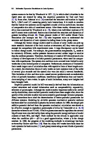
In this paper, we have investigated crystal growth and defect formation processes in SPE based on molecular dynamics (MD) simulations by employing the Tersoff interatomic potential of Si.[3] Although the Tersoff potential gives rise to high melting temperature 2547 K,[4] it can well reproduce the structural properties of a-Si[5] and liquid Si[6], and thus it is considered to be useful to describe crystallization as well as defect formation processes during SPE of Si. METHOD MD simulations have been performed using a MD cell including an a/c interface. The typical MD cell size is 21.7x21.7x43.4A 3 (tetragonal prism) and the number of Si atoms, 1024 was determined by using the crystalline Si density 2.33 g/ cm 3 . Atomic movements were determined by solving Langevin equations rn',(t) = F, (t) - rnyt',(t) + Rf t), (1) where m is the atomic mass, ri(t) the position vector of the i-th atom at time t, Fi(t) the interatomic force calculated by the Tersoff potential, and y and Ri(t) are the friction constant and random force to control temperature, respectively. We employed the scheme developed by Gusteren and Berendsen for numerical integrations of the Langevin equation.[7] The time step for the integration was set at 0.001 ps and the friction constant y was chosen to be 5 (ps)-1 . The initial a/c interface was prepared by attaching 8 c-Si(001) layers to a block of bulk a-Si obtained by rapid quenching of liquid Si.[5] The MD cell was pre-annealed at 1000K for 20ps and then heated at various temperatures between 1450 and 2000K for crystallization at the a / c interface. In order to examine atomic motions during SPE growth, atomic coordinates contained in the central region including the diagonal (110) plane of the tetragonal cell with a thickness of 10A were projected on the (110) plane. In order to investigate defect formation processes during SPE, we have utilized a larger MD cell with a size of 65.1x65.1x43.4A 3 made by combining the nine small MD cells described above. RESULTS AND DISCUSSIONS Growth Mechanism Figures 1(a) shows an example of the typical SPE processes obtained by MD simulations at 2000K. These simulations indicated that the a/c interface was rough for the temperatures larger than 1600K, while it was rather flat for the temperatures less than 1550K. Figure 1(b) shows a magnified view of the part enclosed by the squares in Fig. 1(a). From Fig. 1(b), it is suggested that a stable 1111) facet is formed at the a/c interface as 264
Ops
(a)
550ps
SlOOOps
750ps
6050o 40.
.K 3020ý
10 0
10
20
30
X(A)
550ps
(b)
617ps
750ps
25 20 15
10 5
0 0
5
10 15 20 25
X(A)
Fig. I Typical MD simulation results of SPE growth at 2000K for 1000 ps (a) and a magnified view of the part enclosed by the squares (b).
i
oil
1 ns
12 ns
44 ns
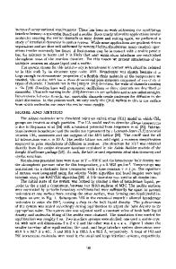
Fig. 2 Typical snapshots of atomic movements during SPE growth at 1450K. 265
Temperature (K)
shown by the dashed lines and the crystal growth along the {111} facet is the rate-limiting step of SPE
Data Loading...


