Near-Infrared Photodetection with Molecular Beam Epitaxy Grown Extended InGaAs
- PDF / 451,632 Bytes
- 6 Pages / 595 x 842 pts (A4) Page_size
- 65 Downloads / 312 Views
FF6.2.1
Near-Infrared Photodetection with Molecular Beam Epitaxy Grown Extended InGaAs Jun-Xian Fu1, Xiaojun Yu, Yu-Hsuan Kuo, and James S Harris, Jr. Department of Applied Physics, Solid State and Photonics Laboratory, Stanford University, Stanford, CA 94305-4075, U.S.A.
1
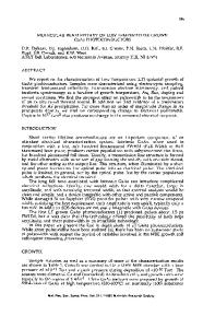
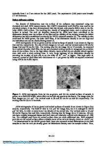
ABSTRACT Strain-balanced InxGa1-xAs/InyGa1-yAs superlattices and fractional monolayer In0.532Ga0.468As/InAs superlattices were grown by solid-source molecular beam epitaxy (SSMBE) in order to extend the photodetection wavelength range beyond 1.7µm. Material qualities were characterized by transmitted electron microscope (TEM), X-ray diffraction (XRD), roomtemperature photoluminesecence (RTPL) and optical absorption measurement. INTRODUCTION The near-infrared wavelength range is of extensive interest for hyperspectral sensing, laser radar, environment gas monitoring and next-generation optical communications. Latticematched InP/InGaAsP based material systems have provided the foundation for state-of-the-art optical communication devices. Standard lattice-matched InGaAs to InP has 53.2% indium and covers the wavelength range up to 1.7µm, while extended InGaAs (with indium composition more than 53.2%) can extend the wavelength range to 1.8-2.5µm, a region of far more spectral interest for remote sensing [1]. Misfit dislocations could be introduced because of the lattice constant difference between the InP substrate and the extended InGaAs layer if the layer thickness goes beyond the critical thickness. The dependence of critical thickness on film strain varied for different growth conditions [2]. It is possible to grow thin film layer with effective thickness over the critical thickness limit by applying specific growth techniques [3,4]. Compared to metamorphic growth of lattice relaxed material, pseudomorphic growth of highly strained film had better misfit dislocation control and been proven appropriate for specific device applications [5]. MATERIAL GROWTH All the samples were grown in a GEN II SSMBE system which has one indium cell, one aluminum cell and two gallium cells as well as an arsenic cracker and a GaP decomposition cell. The growth rate and film layer composition were pre-calibrated. Reflective high energy electron diffraction (RHEED) was used to monitor the layer growth to insure the 2-dimension layer by layer growth mode even for highly strained layers. The surface roughness could be roughly insitu estimated. Growth conditions could be adjusted in order to get smooth interface between different layers. The surface oxide blow-off process in phosphorous overpressure environment was monitored by RHEED (2×4) surface reconstruction patterns. An InP buffer layer was usually first grown with V/III ratio close to ten and the growth rate of 0.5µm/hr. After the buffer layer growth, the substrate was cooled down to room temperature and the GaP decomposition cell was cooled down as well. The growth chamber was pumped for at least half an hour to reduce the residual effect of phosphorous on the growth of arsenide layer. A lattice-matched layer
Data Loading...