Numerical Simulations of Microstructural Evolution of Lamellar Alloys: Applications to Pb-Sn Solder
- PDF / 900,608 Bytes
- 6 Pages / 612 x 792 pts (letter) Page_size
- 89 Downloads / 359 Views
Numerical Simulations of Microstructural Evolution of Lamellar Alloys: Applications to Pb-Sn Solder Rifa J. El-Khozondar1, Vitcheslav S. Solomatov1 and Veena Tikare Materials Modeling and Simulation, Sandia National Laboratories, MS 1405, Albuquerque, NM 87185, U.S.A. 1 Department of Physics, New Mexico State University, P.O.Box 3001, Las Cruces, NM 88003, U.S.A. ABSTRACT Understanding the morphological changes of Pb-Sn solder alloys helps to improve their performance in electronic applications. The focus of our study is degeneration of lamellar structures at high temperatures. Microstructural evolution of the Pb-Sn eutectic lamellar structure is modeled numerically using Monte Carlo Potts approach. The initial structure consists of alternating layers of Pb-rich and Sn-rich phases, simulating the lamellar array in a near eutectic system. Faults are introduced to destabilize the system. After a short incubation period the shape of lamellae become irregular. The perturbations grow with time and eventually break the lamellae into nearly equiaxed grains. The grain size of the degenerated structure is 2-3 times the original lamellar spacing weakly depending on the spacing between the faults. This is consistent with the experimental observation of degeneration of Pb-62 wt% Sn solder. The duration of degeneration processes is comparable with the time it would take Ostwald ripening to produce grains of the same size. Eventually grain growth reaches the asymptotic regime of coarsening described by a power-law function of time.
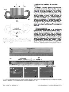
INTRODUCTION Pb-Sn solder alloys have wide applications in most electronic products. Pb-62 wt% Sn eutectic alloy is commonly used to join several metallic parts in electronic packages. The solder joints experience thermal fluctuations due to changes in ambient temperatures, or heat dissipations in electronic components. Thermal fluctuations and turning the power on and off cause cyclical strains and stresses in solder joints. These result from thermal expansion coefficient mismatches between different components of the package. These conditions lead to thermal fatigue failure of solder joints [1]. Several studies concentrated on understanding the thermal failure of solder joints with the goal of being able to develop reliable materials in electronic components. Frear et al. [2] observed that heterogeneous coarsened regions developed throughout the near-eutectic Pb-Sn solder during strain in thermal cycling. The failure initiated in the Sn-rich phase, within the coarsened regions. Cracks then formed across the Pb-rich phase after the Sn phase failed. It was supposed that cracks were only observed throughout the coarsened region because large grains in the coarsened regions can no longer rotate and slide to accommodate the strain. Therefore, the microstructural evolution is related to the failure in solder joints [3]. The microstructure is an important factor in the rate-controlling deformation mechanism. For example, faster cooling rates of near-eutectic Pb-Sn alloy produce degenerate eutectic structur
Data Loading...