Ohmic Contacts to p-Type InGaAs/InP with a Graded Bandgap Heterobarrier
- PDF / 1,158,981 Bytes
- 6 Pages / 414.72 x 648 pts Page_size
- 41 Downloads / 300 Views
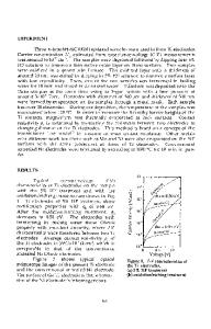
ABSTRACT Ohmic contacts to p-type InP with an In 0.47Ga 0.53As buffer layer and an interposed superlattice of 50)A In 0 .47Ga0 .53 As/ 50 A InP have been investigated. Initial studies of contacts to In0 .47Ga0 .53 As/ InP without the superlattice structure have shown that Pd/Zn/Pd/Au metallization produced a lower specific contact resistance (p. = 1.1 x 10⁻⁴ Q cm 2 ) than Pd/Ge/Au, and over a wider range of anneal temperature than Au/Zn/Au. The incorporation of the superlattice in the pIn0 .47Ga 0.53As/ InP structure resulted in Pd/Zn/Pd/Au contacts with p, of 3.2 x 10⁻⁵ Q cm 2 asdeposited and 7.5 x 10⁻⁶ 0 cm2 after a 500 TC anneal. The presence of Pd/Zn in the metallization was shown as important in reducing pc. Significant intermixing of the metal layers and In0 .47Ga 0 .53 As occured at >_350 'C, as revealed by Rutherford backscattering spectrometry. INTRODUCTION Ohmic contacts to p-type InP are required in a range of optoelectronic devices including heterostructure lasers, LEDs and PIN detectors. However, low resistance contacts to p-InP have been difficult to fabricate because of the relatively large barrier height at the metal/ semiconductor interface. One approach to the formation of ohmic contacts has been the incorporation of a highly doped layer of small band gap (InxGalxAs) between the metallization and the p-InP. By this method, the metal/ p-InP junction was replaced by two smaller barriers at each of the metal/ InxGalxAs interface and the InxGal1 xAs/ InP heterojunction. As a means of further reducing the barrier height at the heterojunction, Wasserbauer et. al. [1] have reported on the inclusion of a superlattice structure between the InxGalixAs and InP. The superlattice of InxGalxAs/ InP was designed to act as a layer with a digitally graded bandgap, thereby reducing the resistance of the p-isotype heterojunction [1]. The metal/ p-InxGal-xAs interface also contributes to the total resistance of the contact. For non-alloyed ohmic contacts to p-InGalxAs, several metallizations based on an interfacial layer of Pd have exhibited low values of specific contact resistance [2-4]. The Pd based metallizations have also shown advantages of a shallow interfacial reaction, the ability to penetrate native oxides and an improved adhesion compared with the conventional p-type contacts of Au/Zn/Au or Au/Be. In particular, the configuration Pd/Zn/Pd/Au has been successfully used to fabricate low resistance contacts to p-type InxGal.As/ InP [1] following the earlier application of this system to p-GaAs [51 and p-InP [6]. However, Wasserbauer et. [11 al. used the Pd/Zn/Pd/Au configuration only in the as-deposited form, while other studies [5,6] have shown that annealing of the metallization was required in order to enhance the indiffusion of the dopant Zn and to minimize the specific contact resistance. In this paper, several of the variables associated with the fabrication of the metal contacts to p-InxGal-xAs/ InP have been systematically examined for the first time. These include the type of metallization, the pre-t
Data Loading...