Optimization of Growth and Activation of Highly Doped p-type GaN for Tunnel Junctions
- PDF / 89,247 Bytes
- 6 Pages / 612 x 792 pts (letter) Page_size
- 14 Downloads / 254 Views
E11.2.1
Optimization of Growth and Activation of Highly Doped p-type GaN for Tunnel Junctions David B. Nicol1, Ali Asghar1, My Tran1, Dhairya Mehta1, and Ian T. Ferguson1, 2* 1
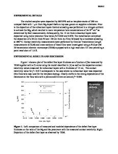
Georgia Institute of Technology, School of Electrical and Computer Engineering, Atlanta, GA 30332-0250, U.S.A. 2 Georgia Institute of Technology, School of Materials Science and Engineering, Atlanta, GA 30332, U.S.A. ABSTRACT Highly doped p-type GaN was grown by MOCVD with a Mg source for use in tunnel junctions for dual wavelength light emitting diodes. Highly doped p-type material (p+) is necessary for creating efficient tunnel junctions that act as buried current spreading layers and provide high quality contacts to p-type GaN. Molar flow ratios and growth temperature were varied to achieve maximum doping concentration. A range of post-growth annealing conditions to activate incorporated Mg was investigated. Secondary Ion Mass Spectrometry (SIMS) and Hall effect were used to measure Mg incorporation and carrier concentration, respectively. The maximum carrier concentration achieved employed a hybrid growth scheme that achieved high carrier concentration and high quality material by alternating layers of high and low growth temperature material. Atmospheric annealing was compared to standard RTA under N2 ambient. Successful GaN tunnel junctions were grown using the hybrid p-type doping scheme developed in this work. I-V measurements were taken on these devices to evaluate the effectiveness of the devices. INTRODUCTION Gallium Nitride (GaN) based materials, with bandgaps ranging from 0.76 eV to 6.20 eV [1], have become very important for many optoelectronic applications. GaN-based light emitting diodes (LED) have fueled a revolution in the lighting industry with the development of new general illumination sources based on LEDs called solid state lighting (SSL) [2]. Other uses for GaN include junction field effect transistors and high electron mobility transistors [3]. While GaN devices have shown much promise, many issues are still being addressed for the optimal solution. One of these is the difficulty in achieving highly doped p-type GaN. High hole concentrations in GaN are difficult to achieve due to the high thermal ionization energy (~180 meV) of Magnesium (Mg) in GaN. At room temperature less than 1% of Mg acceptors are typically electronically active [4]. Therefore, in order to achieve acceptable hole concentrations, high Mg incorporation far above normal doping densities is required. This high doping concentration, however, decreases the crystalline quality of the film, which consequently increases its resistivity and makes it difficult to obtain good electrical contacts to the material. Resistive films cause current crowding in LEDs [5]. A semitransparent contact is deposited onto the entire surface of the p-type region to compensate for current crowding; this is followed by a smaller but thicker bonding pad. The cost of using this semitransparent current spreading layer is a reduction in light extraction from the device by not en
Data Loading...