Photoluminescence and Plane-View Tem Studies of Epitaxial ZnSe Layers on GaAs After H 2 Gas Heat-Treatment
- PDF / 801,080 Bytes
- 6 Pages / 420.48 x 639 pts Page_size
- 45 Downloads / 301 Views
PHOTOLUMINESCENCE AND PLANE-VIEW TEM STUDIES OF LAYERS ON GaAs AFTER H2 GAS HEAT-TREATMENT
EPITAXIAL
ZnSe
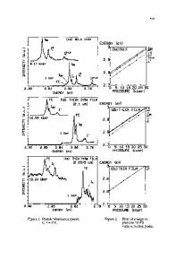
MAKI SEKOGUCHI%, TAKASHI MURASE AND TSUNEMASA TAGUCHI Faculty of Engineering, Osaka University, Suita, Osaka 565, Japan. *Present address, Research Institute of Electrical Communication, Tohoku University, 1-1, Katahira 2, Sendai, Miyagi 980, Japan. ABSTRACT Low-temperature photoluminescence and plane-view TEN observations have been carried out to investigate the strain and microstructural defects in MOCVD-grown ZnSe/(lOO)GaAs after postgrowth annealing in H2 gas at temperature between 350 and 500V. A 0.35gm thick ZnSe epitaxial layer is originally under compressive strain, but after annealing this receives considerably tensile strain, and the neutral deep-acceptor bound exciton (Il) line and the edge-emission band at about 2.72 eV newly appear. The observed changes are interpreted in terms of the energy downshift of the excitonic lines and deviation from stoichiometry. The annealed film, which deteriorated as a result of generations of dislocation tangles and small loops, results in the strong deep-level emissions around 2.25 eV. INTRODUCTION Recently, interest in ZnSe/GaAs heterostructure has centered on the kinetics of strain relaxation [1,2] depending upon film thickness and the thermal stability [3,4] of the epitaxial layers or interfaces. It has been reported so far that the critical thickness for the onset of inelastic strain relief due to the generation of misfit dislocations is about O.15Am and complete relaxation occurs for thicknesses around lm. However, Yao et al. [5] have pointed out that the thermal strain becomes important above lm because significant changes of the valence band structure appear with increasing growth temperature. In our early investigations [3] concerning the photoluminescence (PL) and XPS characteristics of the ZnSe on GaAs grown by low-pressure metalorganic chemical-vapour-deposition (MOCVD), we have already emphasized an importance of the thermal strain which results in tensile strain during heat-treatment in H2 or H2 Se gas. The post-growth annealing is usually considered for a process in which ohmic contact formation and ion-implantation, performed at temperatures above 350t, are necessary. Yodo and Yamashita [4] have very recently shown that the epitaxial layers grown by the atmospheric MOCVD is stable than those grown by lowpressure MOCVD after annealing. In order to investigate the strains and microstructural defects in the post-growth annealed ZnSe layers, we have performed PL and transmission electron microscope (TEN) experiments. This paper describes the effect of heat-treatment at temperature between 350 and 5003t in H2 gas pressure (-20 Torr) on photoluminescence properties at 4.2 K in the low-pressure MOCVD-grown ZnSe on (100) GaAs. We will discuss the strain induced during heat-treatment and also shown the structural defects introduced in the epitaxial films as evidenced by planeview TEN observation. Mat. Res. Soc. Symp. Proc. Vol. 145. ©1989 Materials Research
Data Loading...


