Probing of microvoids in high-rate deposited a -Si: H thin films by variable energy positron annihilation spectroscopy
- PDF / 256,365 Bytes
- 8 Pages / 612 x 792 pts (letter) Page_size
- 109 Downloads / 323 Views
MATERIALS RESEARCH
Welcome
Comments
Help
Probing of microvoids in high-rate deposited a-Si : H thin films by variable energy positron annihilation spectroscopy X. Zou, D. P. Webb, Y. C. Chan, and Y. W. Lam Department of Electronic Engineering, City University of Hong Kong, Tat Chee Avenue, Kowloon, Hong Kong
Y. F. Hu, S. Fung, and C. D. Beling Department of Physics, The University of Hong Kong, Pokfulam Road, Hong Kong (Received 15 May 1997; accepted 13 January 1998)
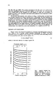
In this paper, positron annihilation measurements have been carried out on a-Si : H thin films deposited by plasma-enhanced chemical vapor deposition (PECVD) at high and low rates by means of the variable energy positron beam Doppler-broadening technique. The depth profiles of microvoids in the films grown under different conditions have been determined. We found a smaller void fraction in the surface region of all films compared to the bulk, and a smaller void fraction in low rate than in high growth rate films. By plotting S and W parameters in the (S, W) plane, we have shown that the vacancies in all of the high-rate and low-rate deposited intrinsic samples, and in differently doped low-rate samples are of the same nature, although there appears to be a higher density of defects in the boron than phosphorus doped films. The depth profiles of the microvoid-like defects in the a-Si : H films are extracted by use of the VEPFIT program.
I. INTRODUCTION
Amorphous tetrahedral semiconductors are important materials for the fabrication of micro- and optoelectronic devices. Advances in this area have, however, been hindered by the limited understanding of their structure, and thus electronic properties, even at the most elementary level. For instance, light-induced degradation of hydrogenated amorphous silicon alloy materials and devices has been the subject of intensive studies, but the origin of the metastability has not been unambiguously identified, and the list of causes includes hydrogen, impurities like C, O, or N, microvoids due to inhomogeneous growth, weak bonds, or a combination of these. Microvoids have also been suggested as metastability centers in a-Si : H, especially in high-rate deposited a-Si : H thin film. Therefore, attention should be focused on microvoid characterization. Using the small-angle x-ray scattering (SAXS) measurement, it has been demonstrated1,2 that even in the best quality material, microvoids of typical diameter 1.0 nm exist, occupying a volume fraction of about 1%. The void density is typically larger for poorer quality material.3 A correlation between the microvoid density in the material with the initial and light-degraded performance of solar cells in which the intrinsic layer has varying microvoid densities caused by changes in the deposition rate has also been established.4 Most defect characterization techniques are not sensitive enough to measure small quantities of point deJ. Mater. Res., Vol. 13, No. 10, Oct 1998
http://journals.cambridge.org
Downloaded: 17 Mar 2015
fects generated during thin film gr
Data Loading...