Production of Sapphire Blanks and Substrates for Blue LEDs and LDs
- PDF / 530,191 Bytes
- 6 Pages / 612 x 792 pts (letter) Page_size
- 79 Downloads / 308 Views
L3.39.1
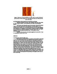
Production of Sapphire Blanks and Substrates for Blue LEDs and LDs Chandra P. Khattak, Frederick Schmid, Paul J. Guggenheim Maynard B. Smith, Henry H. Rogers, and Kurt Schmid Crystal Systems Inc., 27 Congress Street Salem, MA 01970 ABSTRACT The Heat Exchanger Method (HEM) of crystal growing was combined with the Fixed Abrasive Slicing Technology (FAST) to produce low-cost, high-quality sapphire substrates for deposition of the GaN family of compounds. Production quantities of 2-inch diameter blanks have been supplied, and 3-inch diameter material has been qualified. Current technology can be used to prepare sapphire blanks up to 6-inch diameter. INTRODUCTION Gallium nitride (GaN) and related compound semiconductors are among the most attractive materials for blue, violet and ultraviolet light emitting diodes (LEDs), laser diodes (LDs) and high speed, high power transistors [1-3]. Considerable progress has been made with these devices operating with long lifetime and high brightness. A key issue for the growth of GaN has been the lack of a suitable substrate, since GaN substrates are not readily available. While several new substrates, such as AlN [4,5], LaAlO3 [6], LiGaO3 [7] bulk GaN or self-supported film by ELO [8] or Pendeo epitaxy [9], etc., are being explored the most common substrates being used are sapphire (α-Al2O3) and single crystal silicon carbide (SiC). In addition to meeting technical requirements to produce the devices, it is important that the components used in the manufacture be available in large quantities in a manufacturing environment so that lowcost devices can be produced and their full potential realized. Therefore, while novel substrates may find niche applications the real competition is between sapphire and SiC substrates for high volume, widespread use in laser diodes, LEDs and lighting applications. This paper discusses two unique technologies for the production of high quality sapphire substrates in high volume not only to meet current requirements, but also to meet future applications without requiring changes in the basic technologies. These two key technologies are the Heat Exchanger Method (HEM) of crystal growth and the Fixed Abrasive Slicing Technology (FAST) for wafering of sapphire rods. The current requirement of 2-inch diameter substrates is being met in production. However, wafers up to 6-inch diameter size can be produced by modification of production procedures without developing new technologies. HEAT EXCHANGER METHOD The Heat Exchanger Method (HEM) is a solidification technique [10,11] that has been utilized for more than 30 years for growth of sapphire crystals from the melt by controlling the heat input and heat extraction, as shown on Figure 1. A crucible with a single crystal seed centered at the bottom is loaded with sapphire crackle (meltstock) and placed on a hightemperature, helium-cooled heat exchanger. After evacuation of the heat zone, heat is applied and the charge is melted. The seed is prevented from melting by flowing helium gas through the heat
Data Loading...