Properties of Silicon-on-Defect-Layer Material
- PDF / 267,890 Bytes
- 6 Pages / 414.72 x 648 pts Page_size
- 71 Downloads / 648 Views
,
Currently at Institute of Semiconductors, Chinese Academy of
Sciences, Beijing 100083, P. R. China. 745
Mat. Res. Soc. Symp. Proc. Vol. 396 01996 Materials Research Societv
The next generation of very-large-scale-integration (VLSI) circuits fabricated on surface regions of the silicon wafers will require wafers with fewer impurities at the surface; but conventional gettering treatments, which create gettering centers (defect regions) at the center or backside of wafers, are not effective for SOI devices. Thus, enhancement of the gettering efficiency by placing the gettering centers closer to the active area of the device, as in the SODL process, offers a significant advantage for fabricating selectively a high-purity surface layer.
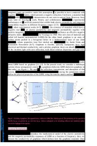
SOI materials are currently produced using separation by implanted oxygen (SIMOX). In this case, high density dislocations are produced in the surface region and high oxygen doses are needed to form the buried isolation layer. Therefore, SODL produced using hydrogen beams may be a useful improvement to this approach since it can be produced with lower doses and has fewer defects at the surface. SODL provides a major cost reduction factor. EXPERIMENT The SODL material was produced following the procedures originally described by Li. 1`3 The silicon wafer was n-type (100) Czochralski (CZ) with a resistivity of about 40 (2-cm cut 00 off axis. The implantation was carried out with H+ion beams at an energy of 180 keV. The beam currents were 120 tA, The beam size was approximately 5 mm, and the dose was 3 X 10¹⁶ protons/cm2 . The wafers were then annealed at 900'C for 10 seconds and 1180'C for 20 minutes. A metal oxide semiconductor field effect transistor (MOSFET) was fabricated on the SODL material. Al was evaporated for the source and drain contacts. SiO+O21 X 10-4Torr) and Cr were evaporated for the gate oxide and gate metal, respectively. RESULTS Spreading resistivity measurements were made after the two annealing steps to define the electrical characteristics of the material. The results, as shown in Fig. 1, indicate that the resistivity of the surface layer has been substantially lowered compared to the value for the bulk material. The maximum of the resistance at the defect layer is estimated to be in the neighborhood of 10' C2. The results corroborate the numerical values given by Ii. 1`3 In addition, note that the implantation causes a change from n-type to p-type material in the surface layer. Although this transformation has been observed previously,5-l" conversion to p-type material is reported here for the first time for SODI. material after two annealing steps. The SIMS measurements shown in Figs. 2 and 3 were done to determine the depth distribution of hydrogen and oxygen in the implanted material. Initial hydrogen distributions were consistent with the predictions
746
10 3
I
NN N NN
102 -
NNN
Np 101
7-
P
_-pp E8 0
€.M
100
pPp
C-
_-
P-
_pPP pp
0D
10"1 PP
10.2
1030 10~
I
P I
TI
IP
I
I
0.5
I
1.0
1.5 Depth (jim)
2.0
2.5
3.0
FIG. 1. Sprea
Data Loading...