Quasi-single Crystal Semiconductors on Glass Substrates Through Biaxially Oriented Buffer Layers
- PDF / 1,191,272 Bytes
- 12 Pages / 612 x 792 pts (letter) Page_size
- 100 Downloads / 303 Views
1268-EE03-06
Quasi-single Crystal Semiconductors on Glass Substrates through Biaxially Oriented Buffer Layers T.-M. Lu1, H. Li1, C. Gaire1, N. Licausi2, T.-L. Chan1, I. Bhat2, S.B. Zhang1, and G.-C. Wang1 1 Department of Physics, Applied Physics and Astronomy 2 Department of Electrical, Computer, and Systems Engineering Rensselaer Polytechnic Institute 110 8th Street, Troy, New York 12180-3590
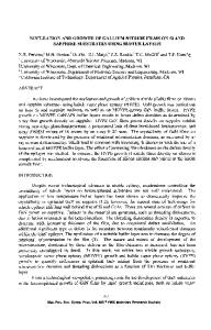
ABSTRACT High efficiency photovoltaic devices are normally fabricated on single crystalline substrates. These single crystalline substrates are expensive and volume production for widespread usage has not been realistic. To date, large volume production of solar cells is on less expensive noncrystalline substrates such as glass. Typically the films grown on glass are polycrystalline with less than ideal efficiency. It was proposed that a dramatic gain in the efficiency may be achieved if one uses a biaxially oriented buffer layer on glass to grow biaxial semiconductor films to fabricate solar devices compared to that of films grown directly on glass. Biaxial films are not exactly single crystal but have strongly preferred crystallographic orientations in both the out-ofplane and in-plane directions. Typically the misorientation between grains can be small (within a few degrees) and may possess low carrier recombination rate. In this paper we shall discuss growth techniques that would allow one to produce biaxial buffer layers on glass. A specific strategy using an atomic shadowing mechanism in an oblique angle deposition configuration that allows one to grow biaxial buffer layers such as CaF2 on glass substrate will be discussed in detail. Results of heteroepitaxy of semiconductor materials such as CdTe and Ge on these biaxial buffer/glass substrates characterized by x-ray pole figure, reflection high energy electron diffraction (RHEED) pole figure and transmission electron microscopy (TEM) will be presented. INTRODUCTION Motivation The most energy efficient solar cells to date are composed of inorganic single crystal semiconductor films grown on single crystal substrates such as Si, Ge, and GaAs [1-3]. Figure 1 shows a summary of the performance of a variety of materials and technology [2]. As can be seen in the plot, typically single crystal materials out-perform polycrystalline or amorphous materials in the same material family. However, from the cost effective point of view, single crystal substrates are too expensive for wide spread solar cell application because solar cells typically require a large area (> 1 m2). This is in contrast to that of
Fig. 1. A summary of solar cell efficiencies for various materials and technologies. Typically single crystal materials out-performed polycrystalline or amorphous materials in the same material family [from ref. 2].
computer microchip applications, which are on the order of 1 cm2. Large volume production of solar cells is still on non-crystalline substrates such as glass [4, 5]. Glass is cheaper but lacks the regular crystalline structure usually necessary to grow high qualit
Data Loading...