Resistance switching behaviors of continuous-thick hBN films fabricated by radio-frequency-sputtering
- PDF / 1,133,072 Bytes
- 10 Pages / 584.957 x 782.986 pts Page_size
- 38 Downloads / 243 Views
Resistance switching behaviors of continuous-thick hBN films fabricated by radio-frequency-sputtering Qiang Li1,2,3 , Xiao Qin3, Qifan Zhang2,3, Yunhe Bai2,3, Hua Tang2,3, Chenyu Hu2, Shuoheng Shen4, Yufeng Li1,2,3, Feng Yun1,2,3,a) 1
Shaanxi Provincial Key Laboratory of Photonics & Information Technology, Xi’an Jiaotong University, Xi’an 710049, China School of Electronic Science and Engineering, Xi’an Jiaotong University, Xi’an 710049, China 3 Solid-State Lighting Engineering Research Center, Xi’an Jiaotong University, Xi’an 710049, China 4 Department of Electronic and Electrical Engineering, University of Sheffield, Mappin Street, Sheffield S1 3JD, UK a) Address all correspondence to this author. e-mail: [email protected] 2
Received: 30 July 2020; accepted: 22 October 2020
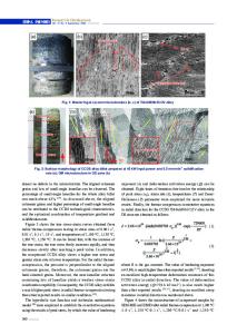
Continuous hBN films have been grown by means of a radio-frequency-sputtering technology, and their material properties have been investigated. The prepared hBN films can achieve good smoothness in a large area. The surface morphologies and compositions of the hBN films on Si substrate and Al film have been characterized, indicating that there is no difference. The 101-phase peak of hBN film is the strongest, and the optical band gap of the fabricated film is 5.84 eV. An attempt on the fabrication of the hBN based resistive switching (RS) device has been made by using an Ag/hBN/Al structure, leading to the observation of a clear and stable RS behavior. The device exhibits a resistance window (high-resistivity state/low-resistivity state) of around 102, and the RS behaviors of hBN film prepared by sputtering were first observed. It has been found that the opening voltage for the device is changed when a different cycle voltage is applied because of the built-in electric field increasing with the increase of applied cycle voltage. The mechanism of the RS behavior has been analyzed, which lay a foundation for the application of hBN as RS material in resistive random access memory to improve the storage density.
Introduction Resistive switching (RS) has been extensively studied due to its wide application in the fabrication of resistive random access memory (RRAM) devices [1, 2]. RRAM has been attracting attention for nonvolatile memory technology owing to its simple structure, high-density integration, low power consumption, fast operation, and strong potential for fabricating multilevel-per-cell memories [3, 4, 5, 6]. The RS devices are typically fabricated in the sandwich structure, namely, an RS layer sandwiched by the metal electrode. By applying bias voltages in excess of given threshold values, the resistivity can be changed from a low-resistivity state (LRS) to a high-resistivity state (HRS) and back [7]. A wide variety of materials exhibiting resistive switching behaviors such as metal oxides, organic polymer, proteins, chalcogenides, and two-dimensional (2D) nanomaterials, have been studied as potential candidates [8, 9, 10, 11, 12]. It is worth highlighting that wide band gap material with high electrical resistivity and hig
Data Loading...