SPA-Leed Measurements on Etched and Polished Silicon (111) Surfaces
- PDF / 911,625 Bytes
- 6 Pages / 417.6 x 639 pts Page_size
- 106 Downloads / 338 Views
Mat. Res. Soc. Symp. Proc. Vol. 54. 1986 Materials Research Society
646
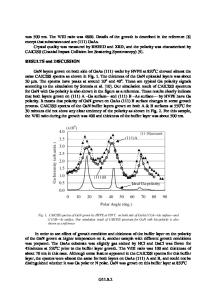
tron Diffraction(RHEED) have been used in the investigation of surfaces and interfaces. This paper presents results on the atomic structure of etched and polished Si(111)-surfaces using SPA-LEED (Spot-Profile Analysis of LEED). METHOD Due to the low energy used in LEED (50-150 eV) the electrons are diffracted at the topmost surface layers of a perfect monocrystal, giving a pattern of sharp spots on the LEED screen at any energy. If steps are present the spot shape changes between sharp (in-phase scattering) and characteristic (out-of-phase) profiles. From this periodic change the step height is derived with high precision [12]. With the help of model calculations [13] the distribution of terraces with respect to orientation, width, and regularity is obtained. Furthermore, point defects at surfaces due to statistical or thermal disorder, domains and superstructures, planar defects like facets and bulk defects like mosaic structures and lattice strain can be identified by characteristic features in the diffraction pattern using strictly the kinematical LEED-theory. This method provides informations about atomic defects strictly within the transfer width of 10 nm by using a common four grid LEED-system or within 100 nm by using a High-Resolution-System respectively. The prospects and limitations of the method are reviewed and discussed in the ref. [12-14]. EXPERIMENTAL The experiments were carried out in a conventional stainless steel UHV-system equipped witp a commercial four grid LEED-system. A base pressure of about 1"10 Pa was sufficient to avoid degradation of the LEED-pattern during a measuring cycle. The wafer samples were dipped into ultra pure HF, which was later on displaced by the addition of methanol. The methanol wets the surface completely and covers it during the transfer into the vacuum. Those surfaces are hydrophobic and almost oxygen free [15]. A special sample handling was used [16] enabling a quick transfer into the UHV. Due to this method we are sure that all features in the LEED-pattern represent properties of the silicon crystal because hydrogen does not interfere. The LEED-spots have been profiled with a CCD-camera, [15] . Specimens were prepared from a 10 ohm-cm for details see ref. B-doped (111) CZ silicon crystal. The wafers were chemo-mechanically polished. RESULTS Atomic structure of etched Si(111)-surfaces Fig. 1 and 2 show scanning electron microscope pictures as well as diffraction patterns of alkaline and acid etched Si(111)wafers. Both surfaces exhibit bright LEED-spots in the Si (lxl)-structure arrangement. The quality of the LEED-pattern indicates that there is no damage at the surface. Changing the electron energy we observe periodically diffuse and sharp spots. The broadening is symmetric indicating that the atomic steps are randomly distributed. The halfwidth as a function of energy is shown in fig. 3 for both surfaces. From the oscillation period [12] we can deduce th t both surfaces exhibit only monoatom
Data Loading...