Atomic Beam Interactions with Silicon (111) Surfaces: A Molecular Dynamics Study
- PDF / 383,681 Bytes
- 6 Pages / 420.48 x 639 pts Page_size
- 13 Downloads / 299 Views
ATOMIC BEAM INTERACTIONS WITH SILICON (ill) SURFACES: A MOLECULAR DYNAMICS STUDY BRIAN W. DODSON AND PAUL A. TAYLOR Sandia National Laboratories,
Albuquerque,
NM 87185
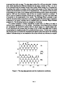
ABSTRACT Low energy (5-20 eV) atomic beam-surface interactions have been studied using a molecular dynamics technique. Silicon atoms are directed at an unreconstructed (111) silicon substrate either perpendicular to the surface or at grazing angles of incidence from 10-35°. The Si-Si interaction is treated using an empirical many-body silicon potential so that the effects of covalent bonding are included. At general beam orientations relative to the surface, low energy atoms are rapidly adsorbed at the surface, whereas at higher energies they either bounce off the surface or penetrate into the substrate. However, when the surface component of beam momentum is parallel to a (100) symmetry direction, Si atoms, under certain conditions, are found to channel along the surface rows, resulting in very little local excitation of the surface geometry and only gradual energy loss. The vertical momentum is carried away by substrate lattice vibrations, and the particle is guided along the surface by interaction with the atoms making up the surface 'half-channels'. This surface channeling effect offers considerable promise for delicate control of the beam-induced annealing/growth of non-equilibrium surface geometries, and thus for high-quality growth at low temperatures.
ADVANCED GROWTH TECHNIQUES Recent developments in the field of semiconductor devices have focused attention on materials with a more critical dependence on physical structure than have traditionally been used. Examples of such structures would include superlattices, one-dimensional geometries, devices with ultrathin layers, such as single quantum wells, and so on. The resulting devices can be very sensitive to the presence of defect structures produced during the growth phase. Since defects often result from depositing materials at high temperatures (especially in compound semiconductors), there is considerable interest in studying processes which may make low-temperature depositions practical. The primary difficulty in low-temperature deposition of semiconductors is the very limited diffusion occurring at low temperatures. This lack of diffusion often results in very defective, or even amorphous, overgrowths. A dilemma thus exists in the use of substrate temperature to fine-tune the quality of deposited material; if the temperature is too low, defects associated with unannealed states will appear, whereas if the temperature is too high, thermally induced (or assisted) defects will limit the film quality. For some systems an adequate window of temperatures exists between these two cases, but this is not always so. To circumvent this problem, work has begun at many laboratories on techniques with the intent of keeping the bulk of the structure relatively cool during deposition and supplying the additional energy needed to grow high-quality material through some external interaction with the s
Data Loading...