Substrate influence on the high-temperature annealing behavior of GaN: Si vs. sapphire
- PDF / 116,354 Bytes
- 6 Pages / 595 x 842 pts (A4) Page_size
- 70 Downloads / 291 Views
0892-FF14-09.1
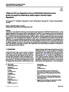
Substrate influence on the high-temperature annealing behavior of GaN: Si vs. sapphire D. Pastor,1 R. Cusc´o,1 L. Art´us,1 E. Iborra,2 J. Jim´enez,3 F. Peir´o,4 G. Gonz´alez-D´ıaz,5 E. Calleja6 1 Institut Jaume Almera (CSIC), C. Llu´ıs Sol´ e i Sabar´ıs s.n., Barcelona, Spain. 2 Tecnolog´ıa Electr´ onica, ETSIT, Universidad Polit´ecnica, Madrid, Spain. 3 F´ısica de la Materia Condensada, ETSII, Universidad de Valladolid, Spain. 4 Dept. Electr` onica, Universidad de Barcelona, Spain. 5 F´ısica Aplicada III, Universidad Complutense, Madrid, Spain. 6 ISOM and Ingenier´ıa Electr´ onica, ETSIT, Universidad Polit´ecnica, Madrid, Spain. ABSTRACT We have studied the effects of rapid thermal annealing at 1300 ◦ C on GaN epilayers grown on AlN buffered Si(111) and on sapphire substrates. After annealing, the epilayers grown on Si display a stained surface. Scanning electron microscopy and optical confocal images revealed the presence of crater-shaped inhomogeneities that develop around protruding nuclei with typically 50 µ m diameter. Energy dispersive x-ray microanalysis yields a high concentration of Si in the crater regions as well as non-stoichiometric concentrations of Ga and N, with an excess of N. Micro-Raman spectra obtained within the crater region exhibit Raman peaks associated with Si3 N4 but no trace of GaN modes, while focused ion beam milling of this region leads to the accumulation of metallic Ga in the etched area. These results suggest that a substantial migration of Si from the substrate takes place during the annealing, which severely alters the material in the crater regions. Such annealing effects, which are not observed in GaN grown on sapphire, constitute a severe drawback for a widespread use of Si(111) substrates when high-temperature processing is required. INTRODUCTION Heteroepitaxy of GaN on Si(111) substrates is an interesting alternative for the fabrication of light emitting diodes (LED) and field effect transistors (FET) because of the availability of large high-quality Si substrates at much lower cost than the sapphire and SiC substrates used for commercially available blue and green LEDs. Also, the development of a nitride-based optoelectronic technology on silicon is highly attractive for integration with the more mature silicon technology [1]. A major problem for the growth of good quality GaN epilayers on Si is the large difference in thermal expansion coefficients, which in the cooling process often leads to cracked layers unsuitable for devices. Also, Si diffusion from the substrate [1, 2] and the formation of an amorphous SiNx layer at the interface [1] contribute to degrade the epilayer quality. The insertion of an AlN buffer is widely used to avoid these problems and to adapt lattice mismatch. In the last few years, the realization of nitride-based blue LEDs [3, 4, 5] and high-electron mobility heterostructures [6, 7] grown on Si(111) has been reported. However, thermal stability of GaN on Si may be an issue when high-temperature processing is required. Decomposition of
Data Loading...