Switching and Negative Capacitance in Thin Amorphous SiC-Si Heterojunction Diode
- PDF / 461,268 Bytes
- 6 Pages / 414.72 x 648 pts Page_size
- 14 Downloads / 226 Views
K. SOHN*, H. LEE* *Department of Electrical and Computer Engineering, New Jersey Institute of Technology, Newark, NJ 07102
ABSTRACT The heterojunction diode of amorphous SiC-pSi with barrier contacts in which the interface layer, a-SiC, is much less than 100 nm and contains considerable defect densities, exhibited bistable
switching with memory. Either state was maintained over weeks without bias. A high-impedance
state switched to a low-impedance state with the transient on-state when a threshold voltage was exceeded. After application of current pulses, a low-impedance switched to a high-impedance state. In C-V Measurement, novel negative capacitance phenomenon in the entire bias range which has not been reported yet was demonstrated. Experimental results show that this negative capacitance is due to the inductive reactance. This phenomenon presents the possibility of replacing inductor even at zero bias. INTRODUCTION In Schottky Diode, under moderate forward bias negative capacitance has been reported in the numerical simulation[1] and observed in the experiment [2]. This phenomenon has been explained by the minority carrier injection and charge delocalization at the interface of metal-semiconductor due to the impact ionization. But, there is still in question about the phenomenon. In our experiment, we observed the negative capacitance in both forward bias and reverse bias with the thin SiC(i) - Si(p) heterojunction diode which has barrier with Al. And it has observed by the Signal Analyzer and LCR Analyzer that phenomenon of negative capacitance is due to the inductive reactance. The Al-amorphous SiC contact formed to the injecting contact due to the high defect density. The carrier injection through the amorphous SiC, which is relaxation semiconductor[3] (i.e., materials for which the dielectric relaxation time exceeds the minority carrier lifetime), may produce the inductance. And, due to the high series capacitance with inductance in both bias, the inductive effect can be dominant. This inductive effect even at zero bias presents the possibility of replacing inductor. In some samples, bistable switching with memory was exhibited in forward bias. The similar type of switching phenomenon has been observed in ZnSe-GaAs, GaP-Ge heterojunction[4]. It was postulated that the switching and
memory behavior is the result of field or impact ionization of traps in a-SiC. THEORY
With a.c. current i, the d.c bias V on injecting contact assuming only drift current, constant electric field, E,
483 Mat. Res. Soc. Symp. Proc. Vol. 318. @1994 Materials Research Society
vi(II
v-S
j-
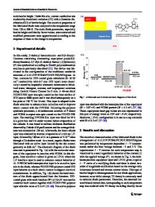
InjectlngT Contact Intrinsic a-SIC
ABarrier Contact
Fig. 1 A a-SiC/Si heterojunction diode i =An(4p)qu,,(P)E
(1)
where An(Ap); the total number of injected electrons (holes) in the a - SiC. p,,(P); the mobility of electrons (holes) using Schockley Theory [5], with sinusiodal small a .c. voltage ve"', the injected electron density is
(2)
ne"'e =(qn, / kT)eq"VIve i where n, electron density in a - SiC V; the d.c. bias voltage V'?1
Data Loading...