The Effect of SiGe Barriers on the Thermal Stability of Highly B-Doped Si Surface Layers
- PDF / 2,377,862 Bytes
- 6 Pages / 612 x 792 pts (letter) Page_size
- 31 Downloads / 352 Views
N4.1.1
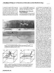
The Effect of SiGe Barriers on the Thermal Stability of Highly B-Doped Si Surface Layers Phillip E. Thompson1, Joe Bennett2, Robert Crosby1, and Mark E. Twigg1 1 Code 6812, Naval Research Laboratory, Washington, DC 20375, U.S.A. 2 International SEMATECH, Austin TX 78741, U.S.A. ABSTRACT We have investigated the use of low-temperature (320 oC) molecular-beam epitaxy (MBE) to form highly conductive, p+, ultra-shallow layers in Si. Although the as-grown B-doped Si is electrically active, in a practical application the doped layers may be exposed to high temperature during post-growth device processing. To minimize the B diffusion, we investigated the use of SiGe diffusion barrier layers. In this work we demonstrate there is less B redistribution with the SiGe diffusion barriers. The use of SiGe diffusion barriers may prove to be critical in the activation of B implants for the formation of ultra-shallow junctions. INTRODUCTION There is a concentrated effort to develop techniques to form ultra-shallow p+ doping layers. For example, gate lengths less than 35 nm are predicted for deep sub-micron complementary metal-oxide-semiconductor (CMOS) field effect transistors [1]. The ideal values for the junction depth of the source/drain regions are only 1/5 to 1/6 of the gate length [1]. In addition, techniques must be developed for the formation of quantum dots, quantum wires, and single electron transistors, as well as for methods to make electrical contacts. While ion implantation is the standard production technique for the formation of p+ contact layers, this procedure may not prove to be an acceptable technique for ultra-shallow junctions due to dopant spread by transient-enhanced-diffusion (TED) [2,3] and boron-enhanced-diffusion (BED) [4,5] after activation by rapid thermal anneal (RTA). Previously we have shown that ultra-shallow p+ layers in Si can be formed using low temperature molecular beam epitaxy (LTMBE) [6-8]. For junction depths of 20 nm or less, the sheet resistance (ohm/square) obtained with LTMBE was an order of magnitude less than that predicted with the use of ion implantation. We have established the thermal budget of the B-doped Si layers so that they may be employed in a device fabrication process [7]. In this article, we present our investigation to increase the thermal stability of the B by growth in ‘thick’ SiGe layers or by the use of SiGe diffusion barriers. EXPERIMENTAL DETAILS The ultra-shallow p-type doped layers were grown by MBE on 75 mm Si (100) Sb-doped (3 – 7 Ω-cm) substrates. The Si and Ge molecular beams were obtained from elemental sources in electron gun evaporators. B was obtained by evaporation of elemental B in a high temperature Knudsen cell. The growth was initiated by heating the Si substrate to 650 oC and then depositing a 50 nm undoped Si buffer layer at 0.1 nm/s. 18 nm of Si was grown while the substrate temperature was lowered to 320 oC, and an additional 18 nm of Si was deposited while the substrate temperature stabilized at 320 oC. The substrate temperature, 320 oC,
Data Loading...