The photosensitivity of a-Si:H/P + Pc-Si heterojunction
- PDF / 176,624 Bytes
- 4 Pages / 420.48 x 639 pts Page_size
- 39 Downloads / 330 Views
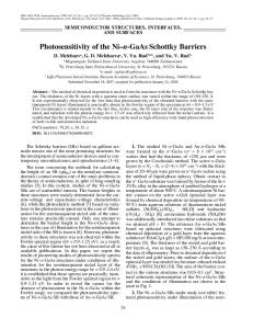
The photosensitivity of a-Si:H/P+Pc-Si heterojunction WANG, WANLU AND LIAO, KEJUN Lanzhou University, Lanzhou, Gansu, China ABSTRACT We have investigated the photosensitivity of the a-Si:H/P+Pc-Si heterojunction. It has been found that the capacitance of a-Si:H/P+Pc-Si heterojunction have an excellent photosensitivity, and potential application as a photosensitive capacitors. Single-crystalline and amorphous heterojunctions have been extensively studied from fundamental theory and their preparation. Their applications, such as wide band-gap emitters, majority carrier rectifiers. High-speed wide band pass photodetectors, beam-of-light transistors, indirect gap injection lasers, and hydrogenated-amorphous silicon carbide (a-SiC:H)/ hydrogenated-amofpho'is silicon (a-Si:H) solar cells have alr5ady shown great potential. 1 -7] M. P. Ali Hideharu Matsuura et al, 8 - ] and other groups have reported on amorphous-crystalline heterojunctions from the viewpoint of understandinq the fundamental device physics. They have presented a systematic study of undoped (n--type) a-Si:H/p-type crystalline silicon (P-c-Si) heterojunction. In this paper, we present results on the photosensitivity of capacitance-voltage (C-V) characteristics of undoped (n--type) a-Si:H/ p-type crystalline silicon (Pc-Si) heterojunctions. It has been found that a-Si:H/Pc-Si heterojunction capacitances have excellent photosensitivity, and potential application as a photosensitive capacitor. The structure of the samples is shown in Fig. 1. The P-type c-Si layer is epitaxially grown on the P+c-Si substrate. The epitaxial film resistivity was 15Qcm, and its thickness 15-17ýim. Substrate values were O.Ol-O.02Qcm and 250vm. The crystal surface used is the (111) face.[lO] The epitaxial crystalline silicon wafers were soaked in a solution of HF to remove Si0 2 , then rinsed in deionized water. Undoped a-Si:H films were deposited by the glow discharge decomposition (GD) of pure siH4 on P+Pc-Si substrates heated to 250°C. A flow rate of 30SCCM and a gas pressure of 89MTorr were maintained during the deposition. The deposition rates were about 1.2A/s for the anode samples. a-Si:H film thickness was 5000-6000A. Aluminium (Al) was subsequently evaporated on an area of Imm 2 of the a-Si:H films in a vacuum of 7xl0- 7 Torr.
Mat. Res. Soc. Symp. Proc. Vol 70. '1986 Materials Research Society
400
OR ITO
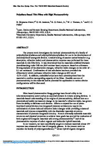
P14URE I Typical C-V characteristics of undoped a-Si:H/P+Pc-Si structure is shown in Fig. 2. C-V characteristics of these samples were measured at lMH2 . With no illumination, its C-V characteristics are very similar to the characteristics of MIS structure at high frequency. Under a microscope lamp, the minimum capacitance, Cmin, gradually increased to the maximum room2 temperature, 20'C.12 The2 minimum with different light intensity at 12 capacitance changed from 30xl0- F/cm to about 122xl0- F/cm with an intensity of 1000 lux which was close to the maximum capacitance (curve F in Fig. 2.).
too
I000wLX E 500
120
D 300 C200
60
B100 A0
-1o
-5
0
5
10
VOLTAGE (
Data Loading...