Photosensitivity of the Ni- n -GaAs Schottky barriers
- PDF / 203,011 Bytes
- 4 Pages / 612 x 792 pts (letter) Page_size
- 73 Downloads / 318 Views
UCTOR STRUCTURES, INTERFACES, AND SURFACES
Photosensitivity of the Ni–n-GaAs Schottky Barriers D. Melebaeva, G. D. Melebaevaa, V. Yu. Rud’b^, and Yu. V. Rud’c aMagtumguly
Turkmen State University, Asgabat, 744000 Turkmenistan Petersburg State Polytechnical University, St. Petersburg, 195251 Russia ^e-mail: [email protected] cIoffe Physicotechnical Institute, Russian Academy of Sciences, St. Petersburg, 194021 Russia bSt.
Submitted December 18, 2007; accepted for publication January 24, 2008
Abstract—The method of chemical deposition is used to form the structures with the Ni–n-GaAs Schottky barrier. The thickness of the Ni layers with a specular outer surface was varied within the range of 150–220 Å. It was experimentally observed for the first time that photosensitivity of the obtained barriers with the semitransparent Ni layers illuminated is practically absent in the Fowler region of the spectrum at hν = 0.9–1.5 eV. This circumstance is related mainly to the fact that, in this case, the Ni layer side of the structure was illuminated, and radiation with the photon energy hν < 1.3 eV was effectively reflected from the nickel surface. It is established that the developed Ni–n-GaAs structures can be used as high-efficiency wide-band photoconverters of both visible and ultraviolet radiation. PACS numbers: 78.20.-e, 81.15.-z DOI: 10.1134/S1063782609010072
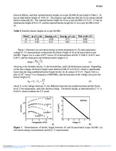
The Schottky barriers (SBs) based on gallium arsenide remain one of the most promising structures for the development of semiconductor devices used in contemporary microelectronics and optoelectronics [1–4]. The issue concerning the methods for calculating the height of an SB (qϕB0) at the metal(m)–semiconductor(s) contact remains one of the main problems in the theory of semiconductors, in spite of long-standing studies [5]. In this context, studies of the Ni–n-GaAs SBs are of undoubtful interest. The barrier heights in these structures were mainly determined from the current–voltage and capacitance–voltage characteristics [6], while the photoelectric method [7] based on variations in the photocurrent spectrum in the case of illumination for the semitransparent nickel side of the structure remains practically unused. Only one attempt to determine the barrier height in the Ni–n-GaAs structures in the case of illumination for the semitransparent nickel side of the SB is known [8]. However, photosensitivity in these structures was not observed within the Fowler spectral region (hν = 0.9–1.25 eV); as a result, the cause of this feature has not been discussed at all in available publications. In this paper, we report the results of pioneering studies of photosensitivity spectra for the Ni–n-GaAs structures under conditions of illumination for the semitransparent nickel layer of the structures in the photon-energy range hν = 0.9–2.4 eV; it is established that these spectra are practically insensitive to the light from the Fowler spectral region hν = 0.9–1.25 eV. In order to reveal the causes for the absence of photocurrent in the Ni–n-GaAs within the Fowler range, we c
Data Loading...