Thin HgCdTe LPE Layers Grown on CdTe and CdZnTe Substrates
- PDF / 1,509,225 Bytes
- 6 Pages / 420.48 x 639 pts Page_size
- 22 Downloads / 354 Views
THIN HgCdTe LPE LAYERS GROWN ON CdTe AND CdZnTe SUBSTRATES KOSAKU YAMAMOTO, TOHRU MAEKAWA and HIROSHI TAKIGAWA FUJITSU LABORATORIES LTD., Infrared Devices Laboratory 10-1 Morinosato-Wakamiya, Atsugi, 243-01, Japan ABSTRACT The dependence of the growth pattern of thin HgCdTe LPE layers on lattice mismatch was investigated. Epilayers grown on substrates with a lattice mismatch of more than 0.2% show island-like growth, which are aligned with the network of misfit dislocation lines. Thin epilayers grown on substrates with a lattice mismatch of less than 0.05% have mirror-like flat surfaces. It was found that the surface defects for thick epilayers also have a lattice-mismatch dependency. INTRODUCTION HgCdTe is a direct band-gap semiconductor with many advantages when used in infrared detectors. Among the crystalgrowth techniques studied, liquid-phase epitaxy is potentially the best process
for producing
HgCdTe
crystals
with
high
crystallinity,
uniformity, and purity. CdTe and CdZnTe are generally used for LPE substrates. CdTe has a 0.2% larger lattice constant than Hg0.8Cd0.2Te. The Cdl-yZnyTe substrate holds promise for lattice matching with Hg 1xCdxTe epilayers [1]. This paper reports the results of our investigation of the dependency of the growth pattern of thin epilayers on lattice mismatch. The island-like growth pattern of thin epilayers is presented, and we propose a model interpreting this growth. We also show how surface defects of thick epilayers depend on lattice mismatch. EXPERIMENT The substrates were (11l)B CdTe and Cdl-yZnyTe. The wafers were cut from an ingot grown by the Bridgman method. The Zn content of Cdl-yZnyTe was measured by atomic absorption
Mat. Res. Soc. Syrmp.Proc. Vol. 130. 1989 Materials Research Society
316
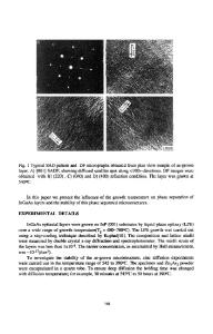
spectroscopy to an accuracy of 3%. Dislocation etch pit density of the CdTe and Cdl-yZnyTe substrates was estimated to be 104-105 cm-2 using the Nakagawa etch [2]. Before epitaxial growth, the substrate surface was etched with a solution of 5% Br in methanol to remove polishing damage. Hg0. 8 Cd 0 . 2 Te epilayers were grown from Te-rich growth solutions using a tipping technique. The epilayers were grown at 480'C with a cooling rate of 0.05°C/min. Surpersaturation of the growth solution was 20 C. RESULTS AND DISCUSSION Figure 1 shows the patterns of thin epilayers grown on different CdTe substrates. The growth times range from 20 to 120 seconds. The epilayer for 120-second growth is about 3 gm thick. Many islands form, grow laterally, become clearly visible, and finally combine. Many dents which are the traces of island boundaries can be seen in Fig. ld.
(a)
(b)
50 pm
(C)
(d)
Figure 1. Photomicrographs of the surface pattern of thin HgCdTe epilayers grown on different CdTe substrates under the following growth times: (a) 20 s, (b) 40 s, (c) 60 s, (d) 120 s. To investigate the cause of this growth, we examined a cross section of the epilayer by etch pitting. Figure 2 shows the cleaved, etched, (110) cross section of an epilayer grown on a CdTe substrate. Note that et
Data Loading...