CdTe Films Grown on InSb Substrates by Organometallic Epitaxy
- PDF / 490,086 Bytes
- 7 Pages / 417.6 x 639 pts Page_size
- 48 Downloads / 341 Views
CdTe FILMS GROWN ON InSb SUBSTRATES BY ORGANOMETALLIC
EPITAXY
I.B. BHAT, N.R. TASKAR, J. AYERS, K. PATEL, AND S.K. GHANDHI Rensselaer Polytechnic Institute, Electrical, Computer, and Systems Engineering Department, Troy, New York 12180
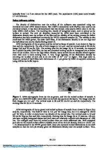
ABSTRACT Cadmium telluride layers were grown on InSb substrates by organometallic vapor phase epitaxy and examined using secondary ion mass spectrometry (SIMS), photoluminescence (Pb) and double crystal x-ray diffraction (DCD). The substrate temperature and the nature of the surface prior to growth are shown to be the most important parameters which influence the quality of CdTe layers. Growth on diethyltelluride (DETe) stabilized InSb substrates resulted in CdTe growth with a misorientation of about 4 minutes of arc with On the other hand, the grown layers followed the respect to the substrates. orientation of the substrates when a dimethylcadmium (DMCd) stabilized InSb was used. Growth at 350 C resulted in the smallest x-ray rocking curve (DCRC) full width at half maximum (FWHM) of about 20 arc seconds. INTRODUCTION The growth of CdTe on InSb has attracted much attention [1-4]
in recent 0
years, because of their close lattice match (better than 0.05% at 25 C). In addition, InSb has higher crystalline perfection than CdTe and is less expensive. It is also available as a large diameter wafer (40mm). We have reported earlier that quality of CdTe grown on InSb substrates by organometallic vapor phase epitaxy (OMVPE) depends on the growth temperature and on the surface quality just prior to growth [5, 6]. In this paper, we report on additional characterization of CdTe layers,prepared under a variety of reactor conditions. The layers were characterized by PL at 10 K, by SIMS, and by double crystal x-ray diffraction. Results of these characterization efforts are used to optimize the growth conditions. EXPERIMENTAL The CdTe films were grown in an atmospheric pressure, horizontal reactor, of the type previously described [5], using diethyltelluride (DETe) and dimethylcadmium (DMCd) as the tellurium and cadmium sources respectively, at 0
growth temperatures from 350 - 420 C. The substrates were (100) 2 0->(l10) oriented InSb, prepolished on one side. The DMCd and DETe partial pressures were 0.5 x 10⁻⁴ atm. and 2 x 10⁻⁴ atm. respectively, and growth times were adjusted so that the layer thickness was approximately 2 pm in each run. PL measurements were made using 7 mW He-Ne laser with a 0.75 meter monochromator and a liquid nitrogen cooled detector with a S-1 photocathode. The x-ray measurements were made with a computer controlled 6" inch double crystal diffractometer (Bede Scientific Instruments Ltd., England) using InSb as the first crystal and Cu K radiation. All x-ray curves refer to (400) reflections. The uniformity of the material was checked by measuring the double crystal rocking curve (DCRC) at different regions in the sample, using an x-y translation stage. The beam incident on the sample was 1mm x 2mm in size.
Mat. Res. Soc. Symp. Proc. Vol. 90. 1987 Materials Research Soci
Data Loading...