Towards Better Understanding of High Efficiency Cd-free CIGS Solar Cells Using Atomic Layer Deposited Indium Sulfide Buf
- PDF / 595,852 Bytes
- 6 Pages / 595 x 842 pts (A4) Page_size
- 99 Downloads / 253 Views
B9.9.1
Towards Better Understanding of High Efficiency Cd-free CIGS Solar Cells Using Atomic Layer Deposited Indium Sulfide Buffer Layers N. Naghavi1, S. Spiering2, M. Powalla2, B. Canava3, A. Taisne4, J.-F. Guillemoles1, S. Taunier4, A. Etcheberry3 and D. Lincot1 1 Laboratoire d’Electrochimie (LECA, UMR 7575 CNRS), Ecole Nationale Supérieure de Chimie de Paris, 11 rue Pierre et Marie Curie, 75231 Paris, France, 2 Zentrum für Sonnenenergie-und Wasserstoff-Forschung Baden-Württemberg, Hessbruehlstrasse 21 C, 70565 Stuttgart, Allemagne 3 Institut Lavoisier (IREM, UMR 8637 CNRS), Université de Versailles-Saint-Quentin, 45 av des Etats Unis, 78035 Versailles, France 4 EDF R&D, Avenue des Renardières, Ecuelles, 77818 Moret-sur-loing Cedex, France ABSTRACT:
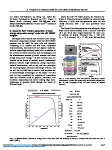
This paper presents optimization studies on the formation of cadmium free buffer layers for high efficiency copper indium diselenide (CIGS) thin film solar cells using a vapor phase route. Indium sulfide layers have been deposited on CIGS substrates by Atomic Layer Deposition (ALD) at substrate temperatures between 140 and 260 °C using indium acetylacetonate and hydrogen sulfide precursors. The parametric study of the deposition temperature shows an optimal value at about 220°C, leading to an efficiency of 16.4 % which is a technological breakthrough. The analysis of the device shows that indium sulfide layers give an improvement of the blue response of the cells as compared a standard CdS processed cell, due to a high apparent band gap (2.7-2.8 eV), higher open circuit voltages (up to 665 mV) and fill factor (78 %) . This denotes high interface quality of the system. Atomic diffusion processes of sodium and copper in the buffer layer are evidenced. INTRODUCTION In high efficiency thin film solar cells based on Cu(In,Ga)Se2 (CIGS) a thin chemical bath deposited CdS buffer layer covers the CIGS layer. Even though the chemically deposited CdS is the buffer layer that yields the best results, there are many advantages to replace it with a wider bandgap material deposited by a vapor deposition process. On one hand a material with a wider bandgap for the buffer layer would lead to higher photocurrent and on the other hand dry processes for heterojunction formation could be better integrated into in-line fabrication. As a soft and highly controllable deposition technique ALD is well adapted for interfacial engineering of thin film based solar cells on indium gallium diselenide (CIGS) [1,2]. This technique is a modified chemical vapor deposition technique based on sequential introduction of reacting precursors into the reactor chamber and allows the deposition of highly homogeneous thin-films with an excellent coverage and layer thickness growth control. In this paper we present further optimization studies allowing to reach a record efficiency of 16.4 % which, to our knowledge, is the best result in this area. Moreover for a better understanding of the In2S3/CIGS junction optical, electrical, structural and compositional characterization of the films have been performed.
Data Loading...